Push-push injection-locking-type frequency multiplier circuit

A frequency multiplier and circuit technology, applied in the field of push-push note-lock frequency multiplier circuits, can solve the problems of narrow operating frequency range, large input signal swing, insufficient output power, etc., and can solve the point of high imaginary impedance. Matching problems, eliminating the use of DC blocking capacitors, and the effect of low input swing requirements

Inactive Publication Date: 2019-04-12
上海奥令科电子科技有限公司
View PDF4 Cites 3 Cited by
  • Summary
  • Abstract
  • Description
  • Claims
  • Application Information

AI Technical Summary

Problems solved by technology

The Gilbert mixing structure is mature, but it needs an orthogonal input signal to suppress the output harmonics; the second harmonic amplifier extracts and amplifies the second harmonic of the transconductance current of the input signal, and the output power is low and the efficiency is low; injection locking The advantage of the structure is low powe

Method used


Image

  • Push-push injection-locking-type frequency multiplier circuit
  • Push-push injection-locking-type frequency multiplier circuit

Examples


Embodiment 1

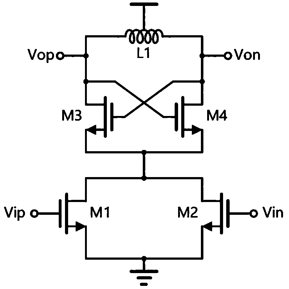
[0019] A push-push note-lock type frequency multiplier circuit, comprising: an input differential pair tube, a cross-coupled pair tube, and an LC circuit; the input differential pair tube is composed of a first NMOS tube M1 and a second NMOS tube M2; the first NMOS tube The drain of M1 is connected to the drain of the second NMOS transistor M2 to form a common drain terminal; the source of the first NMOS transistor M1 is connected to the source of the second NMOS transistor M2 to form a first common source terminal, and the first NMOS transistor M2 A common source terminal is grounded; the gate Vip of the first NMOS transistor M1 and the gate Vin of the second NMOS transistor M2 are connected to a pair of differential input signals; the cross-coupled pair of transistors is composed of the third NMOS transistor M3 and the fourth NMOS transistor M4; The gate of the third NMOS transistor M3 is connected to the drain of the fourth NMOS transistor M4 to form a first gate-drain conne...

Embodiment 2

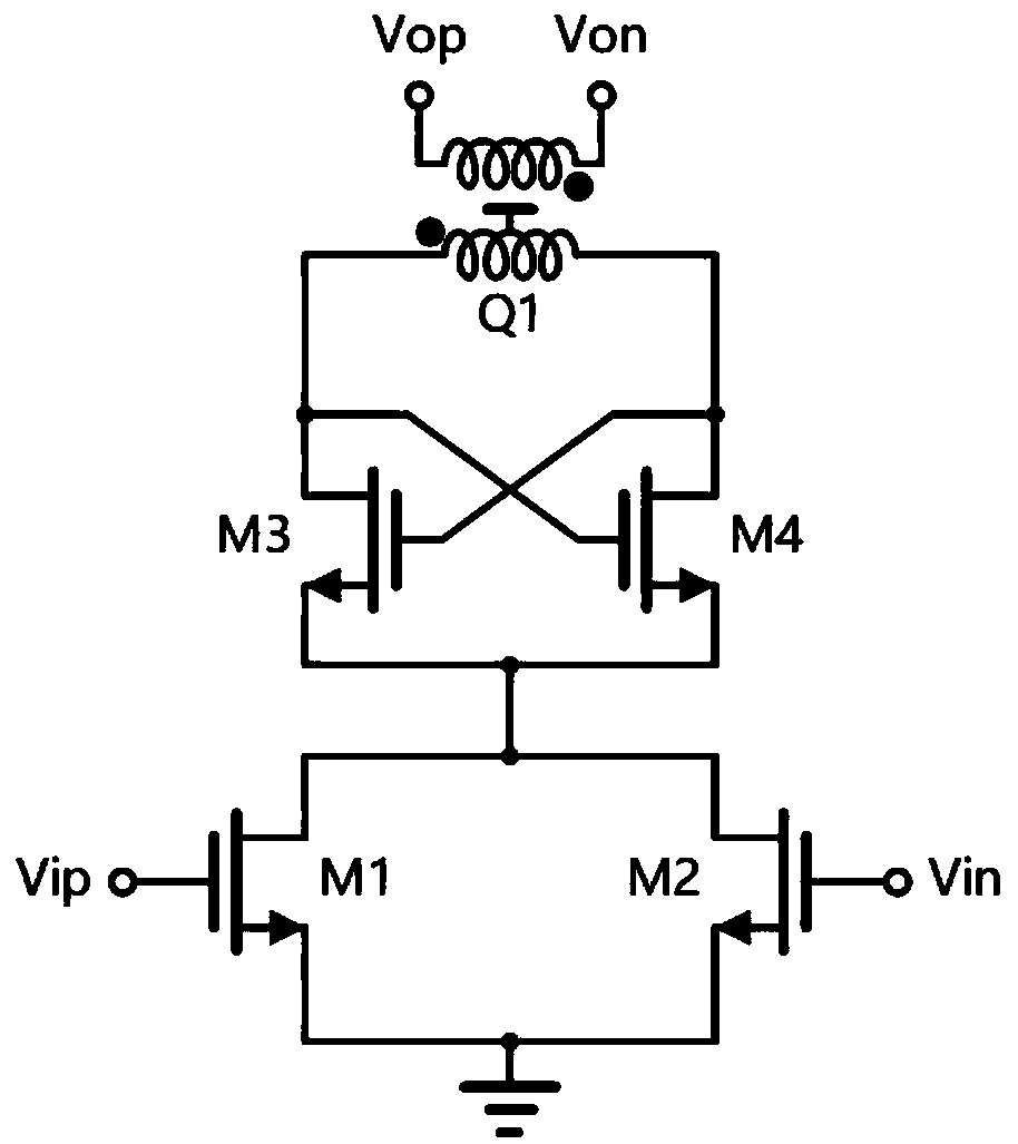
[0022]A push-push injection lock type frequency multiplier circuit, comprising: an input differential pair tube, a cross-coupled pair tube, and a transformer; the input differential pair tube is composed of a first NMOS tube M1 and a second NMOS tube M2; the first NMOS tube M1 The drain of the first NMOS transistor M2 is connected to the drain of the second NMOS transistor M2 to form a common drain terminal; the source of the first NMOS transistor M1 is connected to the source of the second NMOS transistor M2 to form a first common source terminal, and the first The common source terminal is grounded; the gate Vip of the first NMOS transistor M1 and the gate Vin of the second NMOS transistor M2 are connected to a pair of differential input signals; the cross-coupled pair of transistors is composed of the third NMOS transistor M3 and the fourth NMOS transistor M4; The gate of the third NMOS transistor M3 is connected to the drain of the fourth NMOS transistor M4 to form a first ...


PUM


Abstract

The invention discloses a push-push injection-locking-type frequency multiplier circuit. The circuit includes a first NMOS transistor, a second NMOS transistor, a third NMOS transistor, a fourth NMOStransistor and an LC circuit or a transformer. The drain of the first NMOS transistor is connected with the drain of the second NMOS transistor. The source of the first NMOS transistor is connected with the source of the second NMOS transistor, and the common source end is grounded. The gate of the first NMOS transistor and the gate of the second NMOS transistor are connected with a pair of differential input signals. A cross-coupled pair transistor is formed by the third NMOS transistor and the fourth NMOS transistor. The gate of the third NMOS transistor is connected with the drain of the fourth NMOS transistor. The gate of the fourth NMOS transistor is connected with the drain of the third NMOS transistor. The source of the third NMOS transistor is connected with the source of the fourth NMOS transistor. The push-push injection-locking-type frequency multiplier circuit realized in the invention has large output power, and a requirement on input power is also not high, that is, the circuit has the advantages of low power consumption and high efficiency as compared with the prior art.

Description

technical field [0001] The invention relates to the technical field of integrated circuits, in particular to a push-push injection lock type frequency multiplier circuit. Background technique [0002] In recent years, with the continuous evolution of wireless communication 4G and the upcoming commercial use of the fifth-generation mobile communication system 5G, higher data rates require higher frequency bands above 6GHz for communication, such as 28GHz, 39GHz and 60GHz, etc. are gradually included in 3GPP communication in agreement. The high-speed serial data rate in limited communication is also rising, and 28Gbps and 56Gbps have become the mainstream of the industry, and are moving towards a higher rate of 112Gbps. Whether it is wireless or limited communication, a corresponding high-frequency clock frequency is required. VCO is usually used to generate the corresponding frequency, but direct generation of high-frequency VCO often encounters requirements such as process...

Claims


Application Information

Patent Timeline
IPC IPC(8): H03B19/14
Inventor 王昕宇
Owner 上海奥令科电子科技有限公司
Why Eureka
Try Eureka