Wafer preparation method with bumps of different diameters

A technology of bumps and wafers, which is applied in semiconductor/solid-state device manufacturing, semiconductor/solid-state device components, semiconductor devices, etc., can solve problems such as high cost, difficult preparation process, and inability to prepare bumps with different components. High yield and reliability, improved ball drop accuracy, and simple method

Active Publication Date: 2020-12-08
BEIJING MXTRONICS CORP +1
View PDF4 Cites 0 Cited by
  • Summary
  • Abstract
  • Description
  • Claims
  • Application Information

AI Technical Summary

Problems solved by technology

[0005] At present, wafers with bumps of different diameters can only be prepared by electroplating, but the electroplating method cannot realize the preparation of bumps with different components on the same wafer surface, and the preparation process is difficult and costly

Method used


Image

  • Wafer preparation method with bumps of different diameters
  • Wafer preparation method with bumps of different diameters
  • Wafer preparation method with bumps of different diameters

Examples


Embodiment 1

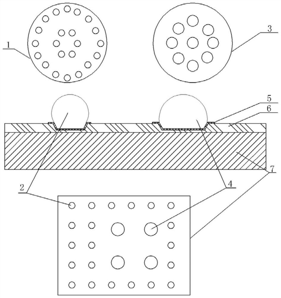
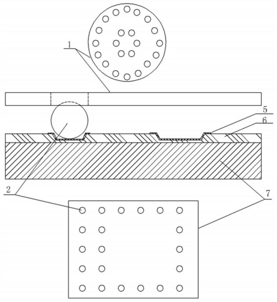
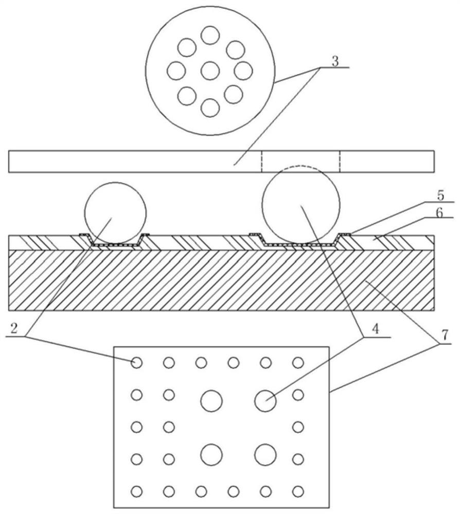
[0045] Such as Figure 2(a) ~ Figure 2(c) As shown, for the case where the bump components are the same, in this embodiment, the under-bump metallization layer is prepared according to the difference in the size of the bumps with different diameters, and then the ball screen with a smaller opening is used to place small-sized solder joints at the required positions. Balls, and then use a large-opening ball-setting screen to place large-size solder balls at the required positions, reflow the wafers with solder balls of different diameters, and complete the bump preparation. Finally, the bumps on the wafer surface are co-processed Face detection. This "drop-drop-back" technological process has a simple implementation method and high work efficiency, yield and reliability. The method specifically includes the following steps:

[0046] (1), preparing the UBM layer 5 at the corresponding position on the insulating layer 6 on the surface of the wafer 7;

[0047] The UBM layer is ...

Embodiment 2

[0059] For the case where the components of the bumps are different, in this embodiment, the solder flux is first printed on the surface of the wafer with the UBM layer prepared, and a small-sized solder ball is placed on the desired position using a ball placement screen with a smaller opening. Wafer reflow is carried out first to complete the preparation of small-size bumps, then flux spraying is performed on the positions of large-size bumps, and then large-size solder balls are missed by using a ball-setting screen with a larger opening, and finally the wafer is reflowed to complete large-size bumps. Bump preparation, this "drop-back-drop-back" process can effectively avoid the impact of the second ball placement on the first placement of the solder balls, and at the same time can realize the preparation of bumps with different components, and can prepare melting point Taller small size bumps, followed by larger size bumps with lower melting points. Specifically include th...


PUM

PropertyMeasurementUnit
thicknessaaaaaaaaaa

Abstract

The invention discloses a method for preparing wafers having bumps with different diameters. The method includes the following steps: for wafers having the bumps with the same composition and different diameters, adopting a small-opening ball placing net plate to complete the placing of a small-sized solder ball first, and then switching to a large-opening ball placing net plate to complete the placing of a large-sized solder ball, and performing uniform refluxing on the whole wafers; and for the wafers having the bumps with different compositions and different diameters, adopting a small-opening ball placing net plate to complete the placing and refluxing of a small-sized solder ball first, and then switching to a large-opening ball placing net plate to complete the placing and refluxingof a large-sized solder ball. According to the scheme of the invention, the bumps with various diameters and different compositions can be prepared on the same wafer by switching the ball placing netplates, and thus the advantages of simple process, high yield and high reliability can be achieved.

Description

technical field [0001] The invention relates to a wafer preparation method with bumps of different diameters, and belongs to the technical field of semiconductor packaging. Background technique [0002] With the continuous improvement of device performance, high density, miniaturization and high reliability requirements are put forward for packaging technology. In order to improve integration and reduce chip size, the size of bumps used in flip-chip packaging is getting smaller and smaller, but small size bumps will cause reliability problems. On the one hand, when the current density is high, the bump diameter is too small , the intermetallic compound inside the bump will accumulate near the anode under the action of electromigration (EM), and generate voids near the cathode, which will cause early interconnection failure; on the other hand, for high power consumption devices, the bump diameter reduction reduces the The path available for heat transfer reduces the heat dis...

Claims


Application Information

Patent Timeline
Patent Type & Authority Patents(China)
IPC IPC(8): H01L23/48H01L23/488H01L23/498H01L21/60
CPCH01L23/48H01L23/488H01L23/49816H01L24/11H01L24/17H01L2224/11
Inventor 谢晓辰刘建松林鹏荣黄颖卓练滨浩黄莹
Owner BEIJING MXTRONICS CORP
Why Eureka
Try Eureka