Thin film transistor and manufacturing method

A thin-film transistor and active layer technology, which is applied in transistors, semiconductor/solid-state device manufacturing, semiconductor devices, etc., can solve the problems of high production cost of metal oxides, achieve excellent stability, resist etching, and save production costs.

Active Publication Date: 2021-05-25
深圳庸行科技有限公司
View PDF0 Cites 0 Cited by
  • Summary
  • Abstract
  • Description
  • Claims
  • Application Information

AI Technical Summary

Problems solved by technology

[0004] In view of this, the present invention provides a thin film transistor and a preparation method to solve the technical problem of high manufacturing cost of the existing metal oxide TFT

Method used


Image

  • Thin film transistor and manufacturing method
  • Thin film transistor and manufacturing method
  • Thin film transistor and manufacturing method

Examples


Embodiment 1

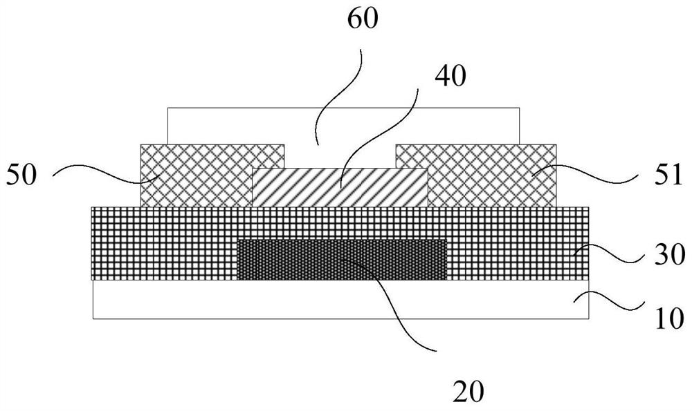
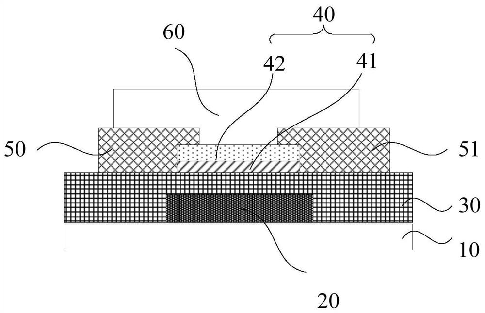
[0035] An embodiment of the present invention provides a thin film transistor. figure 1 A schematic structural diagram of a thin film transistor provided by an embodiment of the present invention. see figure 1 , the thin film transistor includes: a substrate 10; a gate layer 20 formed on the substrate 10; a first insulating layer 30 formed on the gate layer 20; an active layer 40 formed on the first insulating layer 30; The patterned source electrode 50 and the drain electrode 51 on the active layer 40 are electrically connected to the active layer 40 respectively; the organic passivation layer 60 formed on the patterned source electrode 50 and the drain electrode 51, the organic passivation layer 60 is in direct contact with the active layer 40; the active layer 40 includes a metal oxide. Metal oxides including indium oxide In 2 o 3 Composite oxides composed of oxides MO of elements of the fifth subgroup (In 2 o 3 )a(MO) b , wherein, a+b=1, 0.10≤b≤0.50; the organic pas...

Embodiment 2

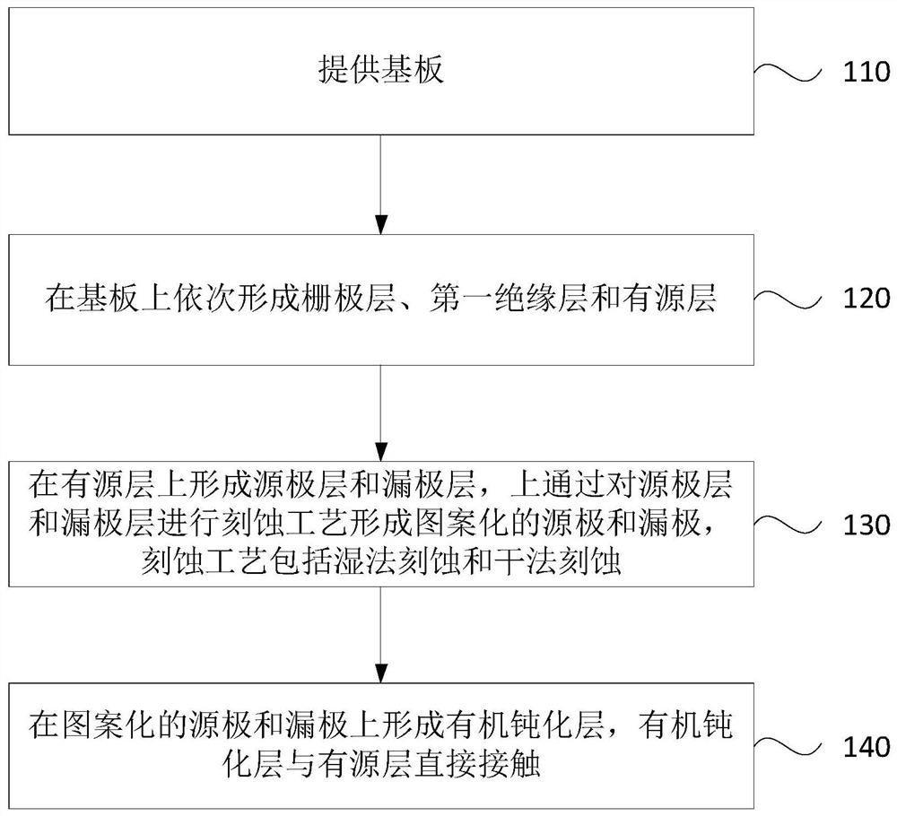
[0053] On the basis of the above-mentioned embodiments, the embodiment of the present invention provides a method for manufacturing a thin film transistor, based on figure 1 thin film transistors shown, see image 3 , the preparation method comprises the steps of:

[0054] Step 110, providing a substrate;

[0055] Step 120, sequentially forming a gate layer, a first insulating layer and an active layer on the substrate;

[0056] Step 130, forming a source layer and a drain layer on the active layer, and forming a patterned source and drain layer by etching the source layer and the drain layer. The etching process includes wet etching and dry etching;

[0057] Step 140 , forming an organic passivation layer on the patterned source and drain electrodes, the organic passivation layer is in direct contact with the active layer; the active layer includes metal oxide. The active layer includes a metal oxide including Indium oxide In 2 o 3 Composite oxides composed of oxides MO...

Embodiment 3

[0097] On the basis of the above technical solution, an embodiment of the present invention provides a display panel, including the thin film transistor mentioned in the above embodiment. Thin film transistors are used to drive display units in display panels.


PUM

PropertyMeasurementUnit
thicknessaaaaaaaaaa
thicknessaaaaaaaaaa
thicknessaaaaaaaaaa

Abstract

The invention discloses a thin film transistor and a preparation method. The thin film transistor comprises: a substrate; a gate layer, a first insulating layer and an active layer formed on the substrate; a patterned source electrode and an active layer formed on the active layer. The drain is electrically connected to the active layer respectively; an organic passivation layer formed on the patterned source and drain, the organic passivation layer is in direct contact with the active layer; the active layer includes metal oxide, metal oxide Including Indium Oxide In 2 o 3 It is a composite oxide composed of oxide MO of the fifth subgroup element, and the organic passivation layer is a polymer organic material. Technical scheme of the present invention, organic passivation layer and indium oxide In 2 o 3 It is in direct contact with the active layer composed of the composite oxide composed of the oxide MO of the fifth subgroup element. On the one hand, the direct contact between the organic passivation layer and the active layer will not cause the effect of donor doping on the active layer, and the device Normal and stable work; on the other hand, the preparation process is simple and the cost is low.

Description

technical field [0001] The invention relates to the technical field of semiconductor materials and devices, in particular to a thin film transistor and a preparation method. Background technique [0002] The core technology of the new flat panel display (Flat Panel Display, FPD) industry is the thin film transistor (ThinFilm Transistor, TFT) backplane technology. Metal oxide TFT (Metal Oxide-TFT, MO-TFT) not only has high mobility, but also has a relatively simple manufacturing process, is compatible with the current a-Si process, has low manufacturing cost, and has excellent large-area uniformity sex. Therefore, MO-TFT technology has attracted the attention of the industry since its birth. [0003] However, due to the relatively "fragile" metal oxide semiconductor film, it is extremely susceptible to the doping effects of non-metallic and metal ions such as acid and alkali etching solutions, plasma, water, oxygen and carbon adsorption, and hydrogen ions. Generally, solve...

Claims


Application Information

Patent Timeline
Patent Type & Authority Patents(China)
IPC IPC(8): H01L29/786H01L21/34
CPCH01L29/66969H01L29/7869
Inventor 徐苗徐华李美灵王磊李民庞佳威陈子楷彭俊彪邹建华陶洪
Owner 深圳庸行科技有限公司
Why Eureka
Try Eureka