Ultrasonic transducer and electronic device
A technology of ultrasonic transducer and electronic device, which is applied in the directions of sound-producing instruments, piezoelectric/electrostrictive/magnetostrictive devices, instruments, etc. Excellent, good working performance, to solve the effect of poor ultrasonic emission capability
- Summary
- Abstract
- Description
- Claims
- Application Information
AI Technical Summary
Problems solved by technology
Method used
Image

Examples
Embodiment 1
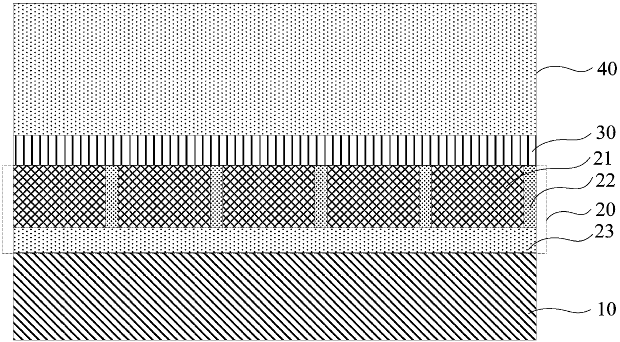
[0056] figure 1 It is a schematic diagram of the cross-sectional structure of the ultrasonic transducer device provided in Embodiment 1 of the present application, figure 2 It is a schematic diagram of the cross-sectional structure of each layer in the ultrasonic transducer device provided in Embodiment 1 of the present application, image 3 It is a schematic diagram of the arrangement of the vibration elements in the ultrasonic receiving layer in the ultrasonic transducer device provided in Embodiment 1 of the present application.
[0057] The ultrasonic transducer device provided in this embodiment can be applied in the field of fingerprint identification, and is used to realize functions such as authorized power-on, access, and credit payment for the current user.
[0058] refer to Figure 1-3 As shown, the ultrasonic transducer device includes: a sensing medium layer 40, an ultrasonic receiving layer 20 capable of receiving ultrasonic waves, and an ultrasonic emitting l...
Embodiment 2
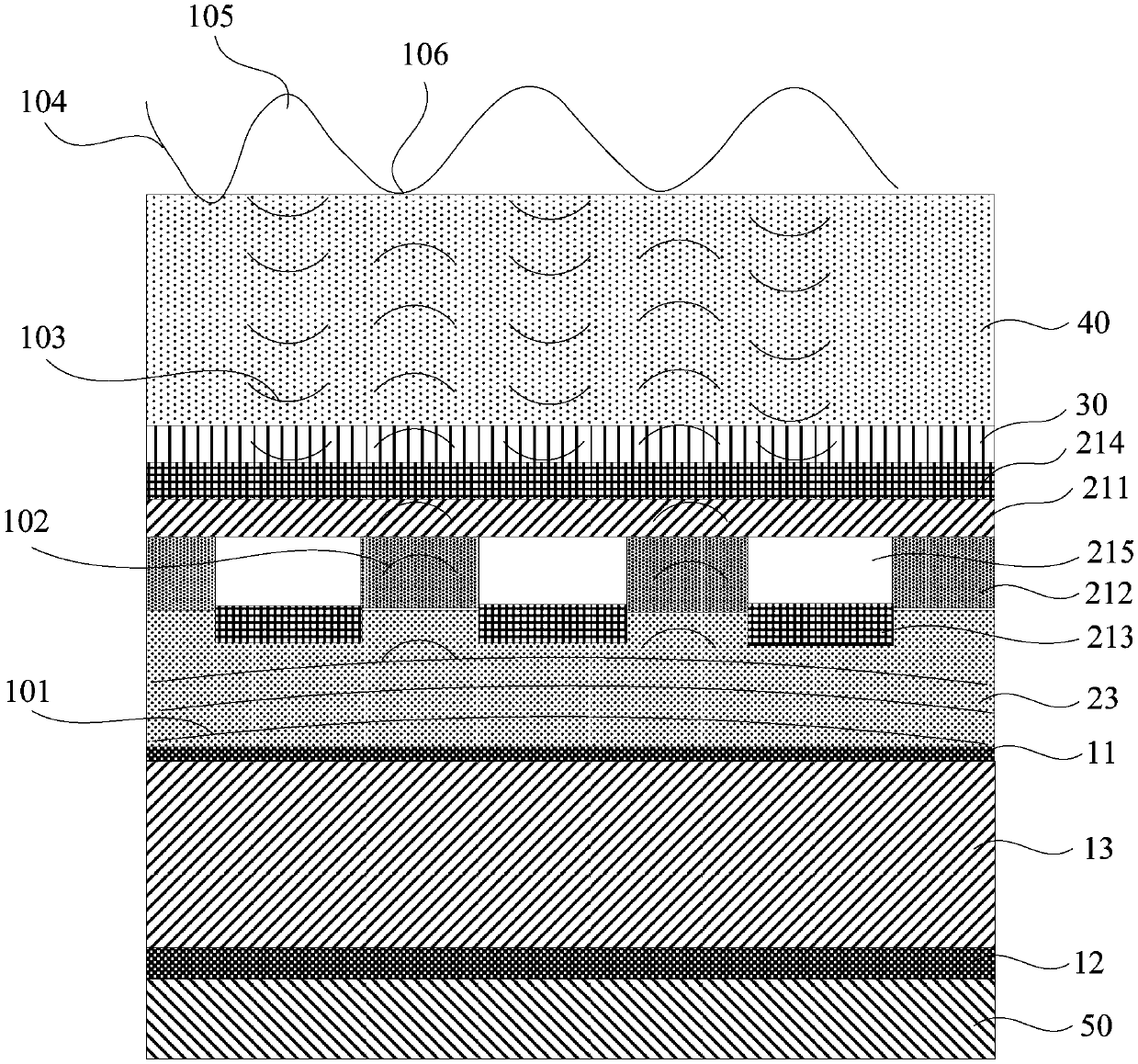
[0078] Figure 4 It is a schematic structural diagram of the cross-sectional structure of each layer in the ultrasonic transducer device provided in Embodiment 2 of the present application.
[0079] The difference between this embodiment and the foregoing embodiments is that in this embodiment, the ultrasonic emitting layer 10 is located between the sensing medium layer 40 and the ultrasonic receiving layer 20, and the ultrasonic receiving layer 20 is located between the backing 50 and the ultrasonic emitting layer 10, The transition layer 30 is located between the sensing medium layer 40 and the ultrasonic emission layer 10 .
[0080] Among them, the working distance of the ultrasonic transducer device provided in this embodiment is specifically as follows: firstly, an alternating electric field is applied between the first electrode layer 11 and the second electrode layer 12 to generate a constant pulsed sound wave 101, when the sound wave reaches the valley of the fingerpri...
Embodiment 3
[0083] Figure 5 It is a schematic structural diagram of the electronic device provided in Embodiment 3 of the present application.
[0084] This embodiment provides an electronic device 100, the electronic device 100 includes the ultrasonic transducer device in any of the above embodiments, wherein the electronic device 100 can be any device that requires feature recognition requirements, such as tablet computers, notebooks, mobile phones or an access control system, etc., wherein, in this embodiment, the electronic device 100 has an ultrasonic scanning area 120 corresponding to the ultrasonic transducer device, and when installed, the sensing medium layer 40 of the ultrasonic transducer device is located in the ultrasonic scanning area 120 or directly It is exposed at the ultrasonic scanning area 120 , and during use, the user's finger can be placed in the ultrasonic scanning area 120 to be recognized by the ultrasonic transducer device.
[0085] Wherein, the electronic dev...
PUM
| Property | Measurement | Unit |
|---|---|---|
| Thickness | aaaaa | aaaaa |
| Thickness | aaaaa | aaaaa |
Abstract
Description
Claims
Application Information
 - Generate Ideas
- Intellectual Property
- Life Sciences
- Materials
- Tech Scout
- Unparalleled Data Quality
- Higher Quality Content
- 60% Fewer Hallucinations
Browse by: Latest US Patents, China's latest patents, Technical Efficacy Thesaurus, Application Domain, Technology Topic, Popular Technical Reports.
© 2025 PatSnap. All rights reserved.Legal|Privacy policy|Modern Slavery Act Transparency Statement|Sitemap|About US| Contact US: help@patsnap.com