Preparation method of improved SiC planar MOSFET device

An improved and device technology, which is applied in the field of preparation of improved SiC planar MOSFET devices, can solve the problems of difficulty in further reducing specific on-resistance and low carrier mobility, etc.

Active Publication Date: 2019-04-19
NO 55 INST CHINA ELECTRONIC SCI & TECHNOLOGYGROUP CO LTD
View PDF1 Cites 1 Cited by
  • Summary
  • Abstract
  • Description
  • Claims
  • Application Information

AI Technical Summary

Problems solved by technology

But the carrier mobility is still very low (generally less than tens of cm 2 ...

Method used


Image

  • Preparation method of improved SiC planar MOSFET device
  • Preparation method of improved SiC planar MOSFET device
  • Preparation method of improved SiC planar MOSFET device

Examples


preparation example Construction

[0024] An improved preparation method of SiC planar MOSFET device includes:

[0025] Prepare an epitaxial layer on the substrate;

[0026] Grow a certain thickness of SiC intrinsic layer on the surface of the epitaxial layer;

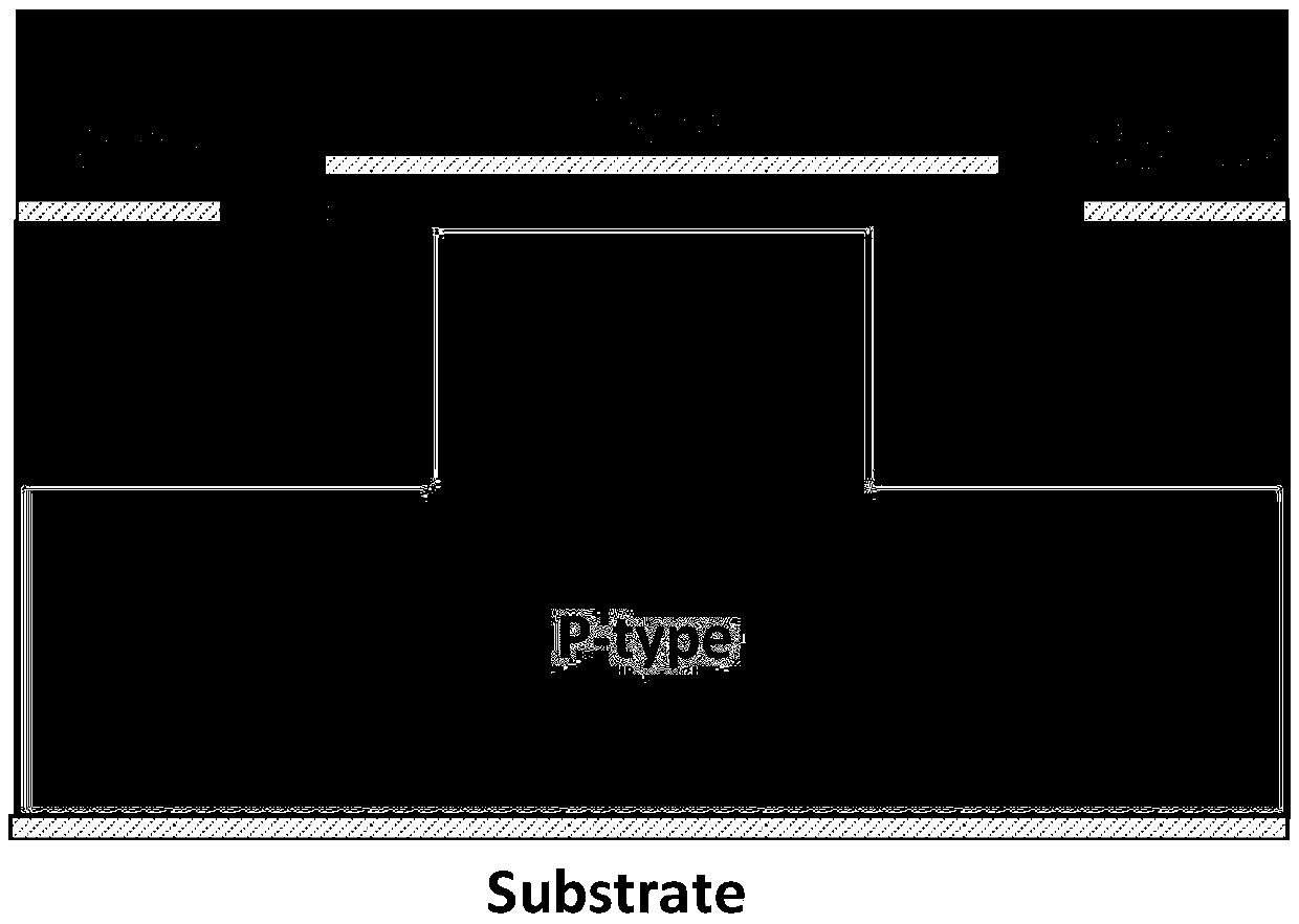
[0027] P-well regions are formed on the surface of the epitaxial layer through mask deposition, photolithography, etching and implantation processes;

[0028] N+ source region is formed by mask deposition, photolithography, etching and implantation processes;

[0029] P+ source contact area through mask deposition, photolithography, etching and implantation processes;

[0030] Forming a gate oxide layer through a thermal oxidation process;

[0031] Polysilicon is formed on the surface of the gate oxide layer through a polysilicon deposition process, and a polysilicon electrode is formed through a polysilicon etching process;

[0032] Depositing the gate-source isolation dielectric, and opening the source contact hole through an etching process;

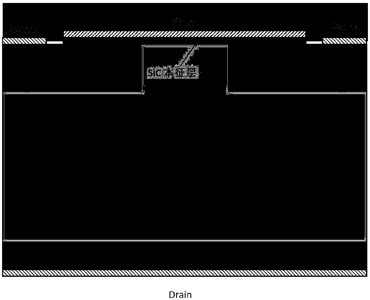
[0033] Metallization...

Embodiment

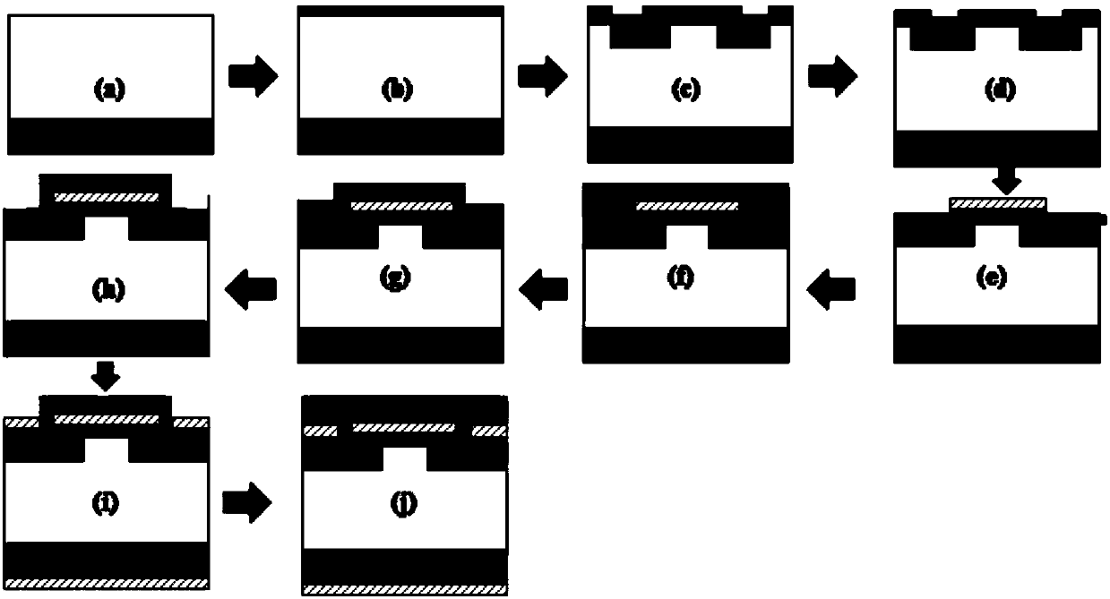
[0046] Such as figure 1 As shown, a method for preparing an improved SiC planar MOSFET device structure includes the following steps:

[0047] (1) Grow an epitaxial layer with a certain thickness on the surface of a heavily doped SiC substrate, such as figure 1 (a) Shown.

[0048] (2) A certain thickness of SiC intrinsic layer is then grown on the surface of the epitaxial layer, such as figure 1 (b) Shown.

[0049] (3) Growing a certain thickness of the implanted mask medium on the surface of the epitaxial layer, and forming such as photolithography, etching and implantation processes figure 1 (c) The mask shape is shown, and P-well ion implantation is performed. The implanted impurities are high-energy Al ions. At the end of the implantation, the mask medium on the surface is removed.

[0050] (4) Growing a certain thickness of the implanted mask medium on the surface of the epitaxial layer, and forming such as photolithography, etching and implantation processes figure 1 (d) The ma...


PUM

PropertyMeasurementUnit
Thicknessaaaaaaaaaa
Doping concentrationaaaaaaaaaa
Thicknessaaaaaaaaaa

Abstract

The invention discloses a preparation method of an improved SiC planar MOSFET device. The improved SiC planar MOSFET device is characterized in that a low-doped epitaxial layer of tens of nanometers is grown on the epitaxial surface of a conventional MOSFET, and the doping concentration is on the order of 1e14cm<3>; the improved MOSFET device structure can greatly improve the width of a channel inversion layer, and can weaken the influence of the high interface state of an SiO2/SiC surface and the doped impurity on the channel mobility, thereby improving the conduction characteristics of the device. The preparation method of the improved SiC planar MOSFET device is conductive to further reduce the device specific on-resistance, and can make a better compromise between device conduction characteristics and blocking characteristics.

Description

Technical field [0001] The invention relates to the field of power semiconductors, in particular to a method for preparing an improved SiC planar MOSFET device. Background technique [0002] Compared with traditional silicon materials, silicon carbide, as a third-generation semiconductor, has a wider band gap, higher breakdown electric field strength and higher thermal conductivity. Power MOSFETs (SiC MOSFETs) based on silicon carbide materials are more suitable for applications in high frequency and high temperature applications. Moreover, the SiC MOSFET can form a surface gate oxide layer through a thermal oxidation process, which is basically compatible with the traditional silicon process. [0003] However, the SiO2 / SiC surface has a high interface state density, which will greatly reduce the mobility of the device channel, increase the channel resistance, and then increase the on-resistance of the device. In recent years, many research institutions at home and abroad have ad...

Claims


Application Information

Patent Timeline
IPC IPC(8): H01L21/04H01L29/78
CPCH01L29/66068H01L29/78Y02B70/10
Inventor 柏松杨同同黄润华
Owner NO 55 INST CHINA ELECTRONIC SCI & TECHNOLOGYGROUP CO LTD
Why Eureka
Try Eureka