Normally-closed gallium oxide field effect transistor structure and preparation method thereof

A gallium oxide field, normally-off technology, used in transistors, semiconductor/solid-state device manufacturing, semiconductor devices, etc., can solve problems such as affecting saturation current and breakdown voltage, uncontrollable etching depth, and unstable threshold value. Achieve the effect of improving device performance, facilitating mass production, and reducing leakage characteristics

Active Publication Date: 2019-04-19
THE 13TH RES INST OF CHINA ELECTRONICS TECH GRP CORP
View PDF4 Cites 7 Cited by
  • Summary
  • Abstract
  • Description
  • Claims
  • Application Information

AI Technical Summary

Problems solved by technology

[0003] The purpose of the present invention is to provide a normally-off gallium oxide field-effect transistor structure to solve the problems of uncontrollable etching depth, etching damage, rough surface, unstable threshold value, serious Technical issues affecting saturation current and breakdown voltage

Method used


Image

  • Normally-closed gallium oxide field effect transistor structure and preparation method thereof
  • Normally-closed gallium oxide field effect transistor structure and preparation method thereof

Examples


Embodiment approach

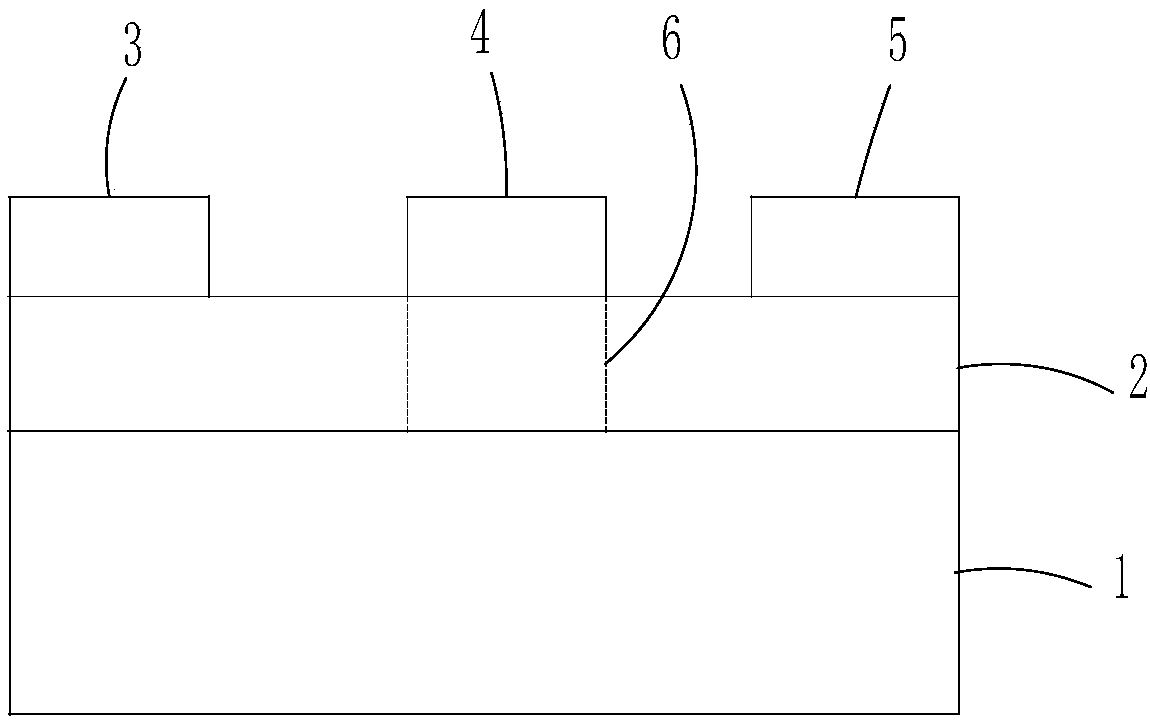
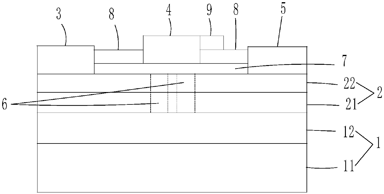
[0031] see figure 1 , as a specific embodiment of the normally-off gallium oxide field effect transistor structure provided by the present invention, the substrate layer 1 includes a sapphire substrate layer 11 and a gallium oxide channel layer 12 from bottom to top.

[0032] see figure 1 , as a specific embodiment of the normally-off gallium oxide field effect transistor structure provided by the present invention, the n-type doped gallium oxide channel layer 2 includes a first n-type doped gallium oxide channel layer 21 from bottom to top and the second n-type doped gallium oxide channel layer 22, the doping concentrations of the first n-type doped gallium oxide channel layer and the second n-type doped gallium oxide channel layer are not equal. The different concentrations of the two layers are beneficial to increase the transconductance of the device and improve the withstand voltage characteristics of the device.

[0033] see figure 1 , as a specific embodiment of the ...


PUM


Abstract

The invention provides a normally-closed gallium oxide field effect transistor structure and a preparation method thereof, and belongs to the technical field of semiconductor devices. The structure comprises a substrate layer and an n-type doped gallium oxide channel layer from bottom to top. A source electrode, a drain electrode and a grid electrode are arranged on the n-type doped gallium oxidechannel layer, and the grid electrode is positioned between the source electrode and the drain electrode, and an electron-free channel region is arranged in the n-type doped gallium oxide channel layer below the grid electrode. According to the invention, the structure does not need a groove to be prepared under a gate, and an electron-channel-free region is formed through high-temperature oxidation, and a gate is formed on the electron-channel-free region, so that the problems of etching damage and uncontrollable etching depth are avoided, and the saturation current and the breakdown voltageare improved.

Description

technical field [0001] The invention belongs to the technical field of semiconductor devices, and more specifically relates to a structure and a preparation method of a normally-off gallium oxide field effect transistor. Background technique [0002] Due to the lack of effective P-type doping and implantation technology, normally-off gallium oxide field effect transistors are usually realized by deep groove technology under the gate, and the groove is generally realized by dry etching. Utilize the deep groove technology under the gate to realize the normally-off gallium oxide field effect transistor device, the etching depth is uncontrollable, and the threshold value is unstable; gallium oxide has strong etching resistance, and dry etching will cause the surface of the groove under the gate Roughness and unevenness will lead to a peak electric field in the area under the gate when the device is working, which will affect the breakdown characteristics of the device. At the sa...

Claims


Application Information

Patent Timeline
Patent Type & Authority Applications(China)
IPC IPC(8): H01L29/10H01L29/40H01L29/78H01L21/336
CPCH01L29/1029H01L29/1033H01L29/402H01L29/66446H01L29/66522H01L29/78H01L29/66969H01L29/7869H01L21/477H01L29/24H01L29/404H01L29/7839
Inventor 吕元杰王元刚周幸叶谭鑫宋旭波梁士雄冯志红
Owner THE 13TH RES INST OF CHINA ELECTRONICS TECH GRP CORP
Why Eureka
Try Eureka