Storage unit manufacturing method and apparatus

A manufacturing method and memory technology, applied in semiconductor/solid-state device manufacturing, electrical components, transistors, etc., can solve problems such as high contact resistance and leakage current deterioration

Inactive Publication Date: 2007-02-21
WINBOND ELECTRONICS CORP
View PDF5 Cites 0 Cited by
  • Summary
  • Abstract
  • Description
  • Claims
  • Application Information

AI Technical Summary

Problems solved by technology

However, directly integrating the above two circuits with different characteristics in the same manufacturing process will cause the following problems: as far as the memory circuit part is concerned, the leakage current of the memory cell and the capacitor must be limited to a minimum amount as much as possible, so that the memory can have a relatively high performance. long hold time
Therefore, the memory circuit part uses doped polysilicon plugs (Doped poly plug) as the conductive circuit of the memory cell contact area and the bit line contact, providing low leakage junction characteristics, but there is a problem of high contact resistance (Rc)
On the other hand, the logic circuit part of the embedded memory must have a high driving current to have a fast response speed, so the internal conductive circuit is made of tungsten plugs to meet the low contact resistance and high-speed characteristics, but the leakage current is relatively worse

Method used


Image

  • Storage unit manufacturing method and apparatus
  • Storage unit manufacturing method and apparatus
  • Storage unit manufacturing method and apparatus

Examples


Embodiment Construction

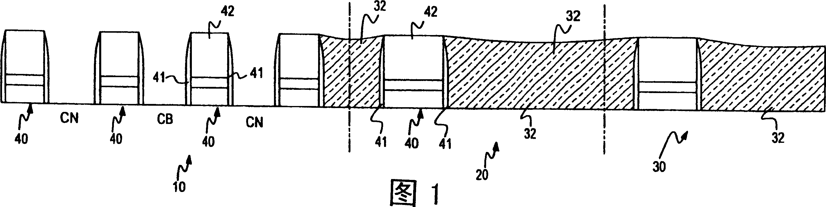
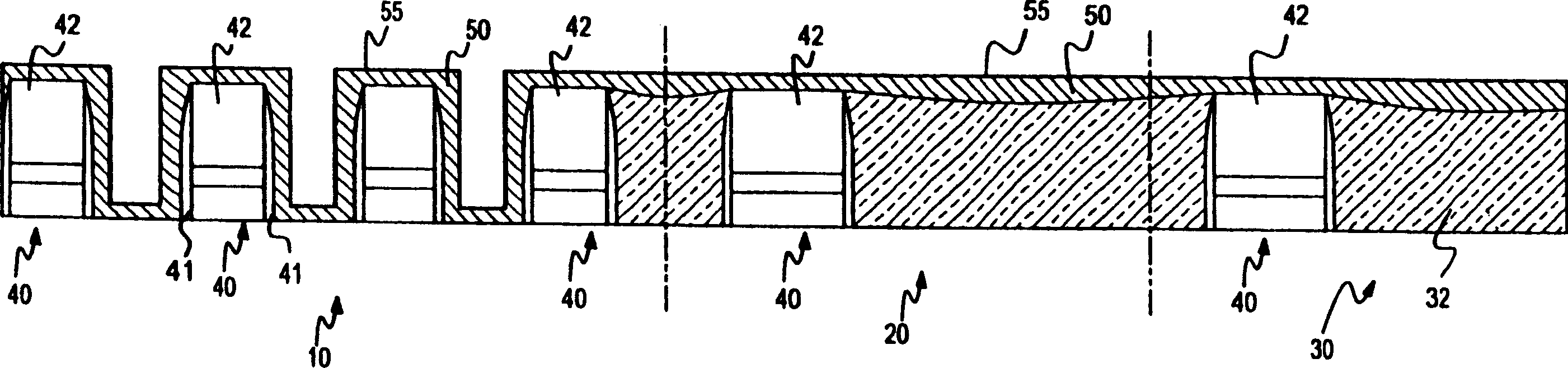
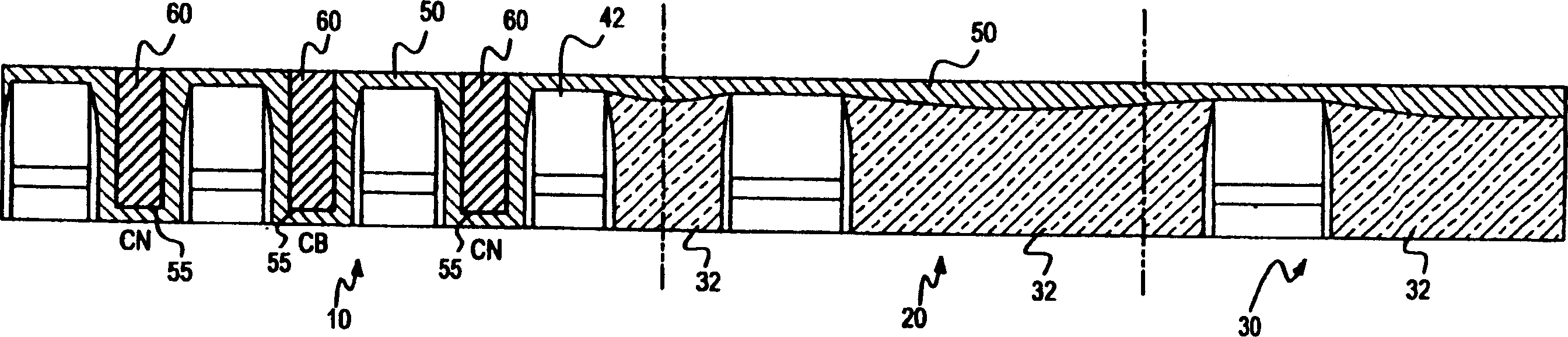
[0018] The main object of the present invention is to form a double-layer plug containing polysilicon layer and tungsten metal in the memory cell area inside the memory, so that the memory cell area has both low leakage and low contact resistance characteristics, and achieves the purpose of improving the speed of the memory. The front-end manufacturing process of forming memory cells and the back-end manufacturing process of forming capacitors, interconnection wires, and passivation layers are not the object of protection of the present invention, so the following descriptions are only briefly described and not repeated.

[0019] Referring to FIG. 1 , it is a schematic cross-sectional view of a memory. Firstly, the substrate area with DRAM memory cell area 10, DRAM peripheral area 20, and logic circuit area 30 is formed on a silicon substrate, wherein the transistors in each area are formed in the substrate through the previous manufacturing process, which can be seen in FIG. 1...


PUM


Abstract

Depositing an adulterated polycrystalline silicon layer at contact nodes inside storage device and contact zones of bit lines forms an interface with low current leakage. Then, tungsten plug with low contact impedance is formed above the said polycrystalline silicon layer. Thus, the plug of storage in dual layer structure possesses both characters of low current leakage and low contact impedance.

Description

technical field [0001] The present invention relates to a memory manufacturing method and device, in particular to a doped polysilicon layer deposited at the internal contact node of the memory to form a low leakage interface, and then a low contact resistance tungsten plug is formed on the polysilicon layer. The plug constitutes a memory manufacturing method and device for a memory plug having both low leakage current and low contact resistance. technical background [0002] Embedded DRAM (Embeded DRAM) is a kind of DRAM manufactured by integrating memory circuit and logic circuit in the same manufacturing process. However, directly integrating the above two circuits with different characteristics in the same manufacturing process will cause the following problems: as far as the memory circuit part is concerned, the leakage current of the memory cell and the capacitor must be limited to a minimum amount as much as possible, so that the memory can have a relatively high perf...

Claims


Application Information

Patent Timeline
Patent Type & Authority Patents(China)
IPC IPC(8): H01L21/8242H01L27/108
Inventor 黄文魁陈锡铨
Owner WINBOND ELECTRONICS CORP
Why Eureka
Try Eureka