Manufacturing device of multilayer stacked structure and manufacturing method of thin film capacitor
A technology of film capacitors and manufacturing methods, applied in the direction of film/thick film capacitors, capacitor manufacturing, laminated capacitors, etc., can solve the problems of low dielectric constant and complex overall structure, and achieve the effect of improving the dielectric constant
- Summary
- Abstract
- Description
- Claims
- Application Information
AI Technical Summary
Problems solved by technology
Method used
Image

Examples
no. 1 example
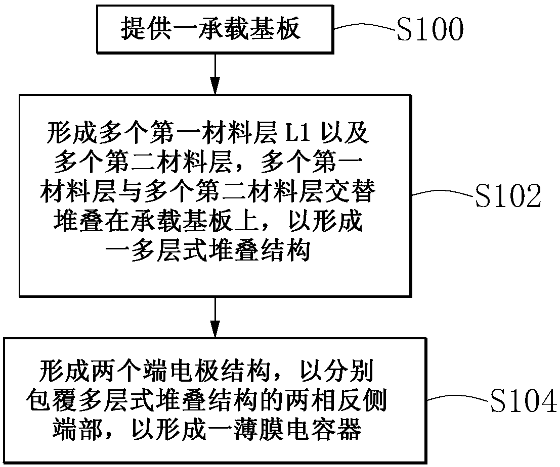
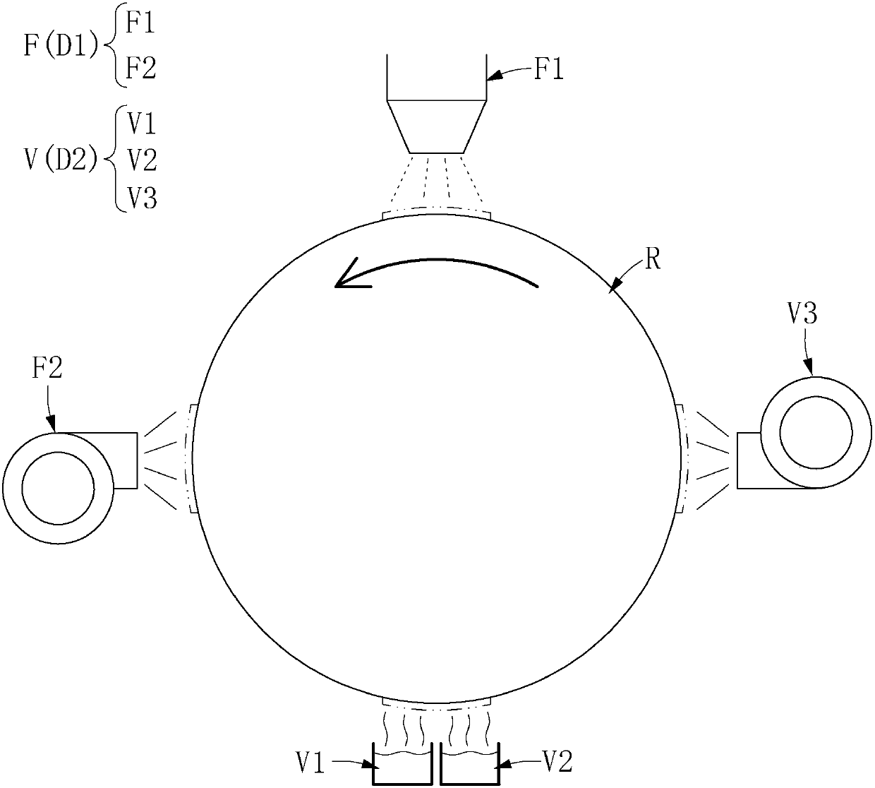
[0034] see Figure 1 to Figure 8 As shown, the first embodiment of the present invention provides a multi-layer stacked structure manufacturing equipment, which includes: a rotatable carrier R, a first material layer forming device D1 and a second material layer forming device D2.
[0035] Furthermore, the rotatable carrier R can be used to carry a carrier substrate 10, the first material layer forming device D1 is disposed adjacent to the rotatable carrier R, and the second material layer forming device D2 is adjacent to the rotatable carrier R. set up. In addition, a plurality of first material layers L1 can be formed by the first material layer forming device D1, a plurality of second material layers L2 can be formed by the second material layer forming device D2, and the first material layer forming device D1 and the second material layer One of the layer forming devices D2 is a co-evaporation device V. In addition, the co-evaporation device V can simultaneously provide ...
no. 2 example
[0049] see Figure 11 to Figure 16 As shown, the second embodiment of the present invention provides a manufacturing equipment of a multi-layer stacked structure and a manufacturing method of a film capacitor. Depend on Figures 11-16 and Figure 2-7 It can be seen that the biggest difference between the second embodiment of the present invention and the first embodiment is:
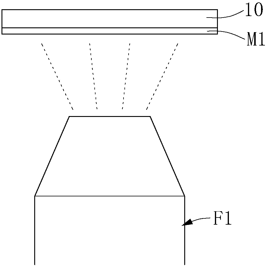
[0050] First, in the second embodiment, the first material layer L1 can be an insulating material layer 12 mixed with a plurality of conductive particles 120 inside, and the second material layer L2 can be a metal material layer 11 . In addition, the first material layer forming device D1 can be a co-evaporation device V, and the second material layer forming device D2 can be a metal material layer forming device F for forming the metal material layer 11 . In addition, the insulating material layer 12 can be formed by the insulating material M2 provided by the co-evaporation device V, and the conducti...
PUM
 Abstract
Description
Claims
Application Information
 - R&D Engineer
- R&D Manager
- IP Professional
- Industry Leading Data Capabilities
- Powerful AI technology
- Patent DNA Extraction
Browse by: Latest US Patents, China's latest patents, Technical Efficacy Thesaurus, Application Domain, Technology Topic.
© 2024 PatSnap. All rights reserved.Legal|Privacy policy|Modern Slavery Act Transparency Statement|Sitemap