LED chip die-bonding method and package method of display module having same

A technology of LED chips and packaging methods, which is applied in the direction of assembling printed circuits, identification devices, instruments, etc. of electrical components, and can solve problems such as short-circuiting of positive and negative electrodes of LED chips

Active Publication Date: 2019-04-23
LEYARD
View PDF3 Cites 2 Cited by
  • Summary
  • Abstract
  • Description
  • Claims
  • Application Information

AI Technical Summary

Problems solved by technology

[0004] The main purpose of the present invention is to provide a method for bonding LED chips and a packaging method for a display module with the same, so as to solve the problem in the prior art that the LED chip bonding process easily leads to a short circuit between the positive and negative electrodes of the LED chip.

Method used


Image

  • LED chip die-bonding method and package method of display module having same

Examples


Embodiment 1

[0038] This embodiment may specifically include the following steps:

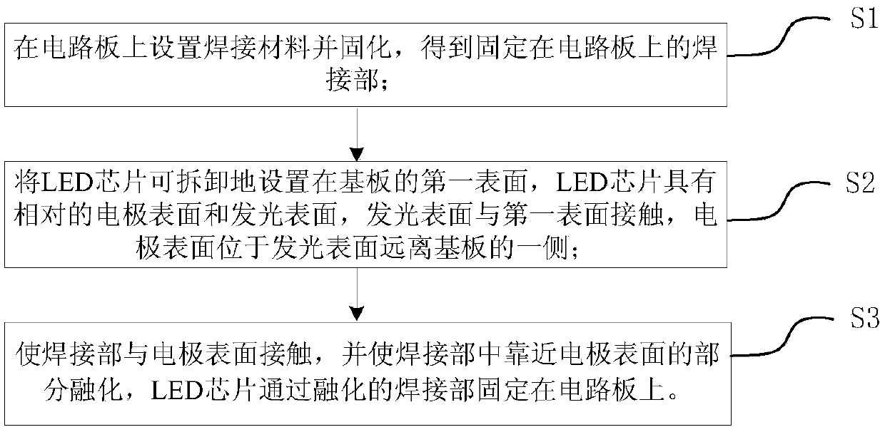
[0039] For the PCB substrate that has been designed and processed, stencil printing is used to print solder paste on the pads that need to be soldered to the LED chip on the PCB substrate. Subsequently, the printed PCB substrate with solder paste is placed in a reflow furnace for high temperature reflow soldering at 200°C. After the process is completed, the top of the solder paste is raised in an arc shape, and the bottom of the solder paste is closely combined with the pad on the PCB substrate.

[0040] A temporary substrate is selected, and the LED chips are arranged on the temporary substrate according to a certain arrangement. A layer of film paper is covered on the temporary substrate. The film paper is sticky on both sides, one side is attached to the temporary substrate, and the other side is attached to the LED chip. A mark, such as a circle or a square, is engraved on the temporary substrate, an...

Embodiment 2

[0045] The difference between this embodiment and embodiment 1 is:

[0046] Place the printed PCB substrate with solder paste in a reflow furnace for high temperature reflow soldering at 130°C.

Embodiment 3

[0048] The difference between this embodiment and embodiment 1 is:

[0049] Place the printed PCB substrate with solder paste in a reflow furnace for high temperature reflow soldering at 270°C.


PUM


Abstract

The invention provides a LED chip die-bonding method and a package method of a display module having the same. The LED chip die-bonding method comprises the steps of: S1, disposing a welding materialon a circuit board for curing to obtain a welding portion fixed on the circuit board; S2, detachably disposing a LED chip on the first surface of the substrate, wherein the LED chip has an electrode surface and a light emitting surface which are opposite, the light emitting surface is in contact with the first surface, and the electrode surface is located on one side, far away from the substrate,of the light emitting surface; and S3, making the welding portion and the surface of the electrode contact, and allowing the portion, close to the surface of the electrode, of the welding portion to be melted, and fixing the LED chip on the circuit board through the melted welding portion. The LED chip die-bonding method cannot pull the LED chip and cannot cause short-circuit of positive and negative electrodes so as to improve the yield of the die-bonding process; and compared to the prior art, the LED chip die-bonding method can perform die-bonding of hundreds of LED chips each time so as toimprove the die-bonding efficiency.

Description

technical field [0001] The invention relates to the field of LED display, in particular to a method for bonding LED chips and a method for packaging a display module having the same. Background technique [0002] The COB package is Chip On Board, which is to adhere the bare chip to the interconnection substrate with conductive or non-conductive adhesive, and then wire bond to realize its electrical connection. The application of COB packaging technology in the field of LED display is becoming more and more extensive. For example, LED die bonding is the specific application of COB packaging technology in the field of LED display. The general process of LED solid crystal process is: first put solder paste or silver glue on the PCB, then pick up the LED chip and place it on the designated position, and finally perform high-temperature reflow soldering, so that the LED chip is soldered to the PCB. . [0003] However, with the development of LED chip technology, in order to fur...

Claims


Application Information

Patent Timeline
Patent Type & Authority Applications(China)
IPC IPC(8): H05K3/34H01L33/62G09F9/33
CPCG09F9/33H01L33/62H05K3/3436H05K3/3494
Inventor 卢长军马莉余杰
Owner LEYARD
Why Eureka
Try Eureka