Device having reverse current-passing function

A device and flow-through technology, which is applied in the field of devices with reverse flow function, can solve the problems of reducing the flow capacity of GCT chips, increasing the difficulty of press-fit structure design, and improving the difficulty of the process, so as to improve the overall reliability, Effect of reducing complexity and improving features

Pending Publication Date: 2019-04-26
TSINGHUA UNIV
View PDF0 Cites 4 Cited by
  • Summary
  • Abstract
  • Description
  • Claims
  • Application Information

AI Technical Summary

Problems solved by technology

However, anti-parallel diodes will introduce stray parameters in the circuit, causing peak overvoltage, and will increase the difficulty of designing the press-fit structure. Manufacturing diodes in non-GCT areas will reduce the current flow capacity of the entire GCT chip, and will also Improve the difficulty of process realization, which has a great impact on the yield

Method used


Image

  • Device having reverse current-passing function
  • Device having reverse current-passing function
  • Device having reverse current-passing function

Examples


Embodiment Construction

[0028] In order to make the purpose, technical solutions and advantages of the embodiments of the present invention more clear, the technical solutions in the embodiments of the present invention will be clearly and completely described below in conjunction with the accompanying drawings in the embodiments of the present invention. Obviously, the described embodiments It is a part of embodiments of the present invention, but not all embodiments. Based on the embodiments of the present invention, all other embodiments obtained by persons of ordinary skill in the art without making creative efforts belong to the protection scope of the present invention.

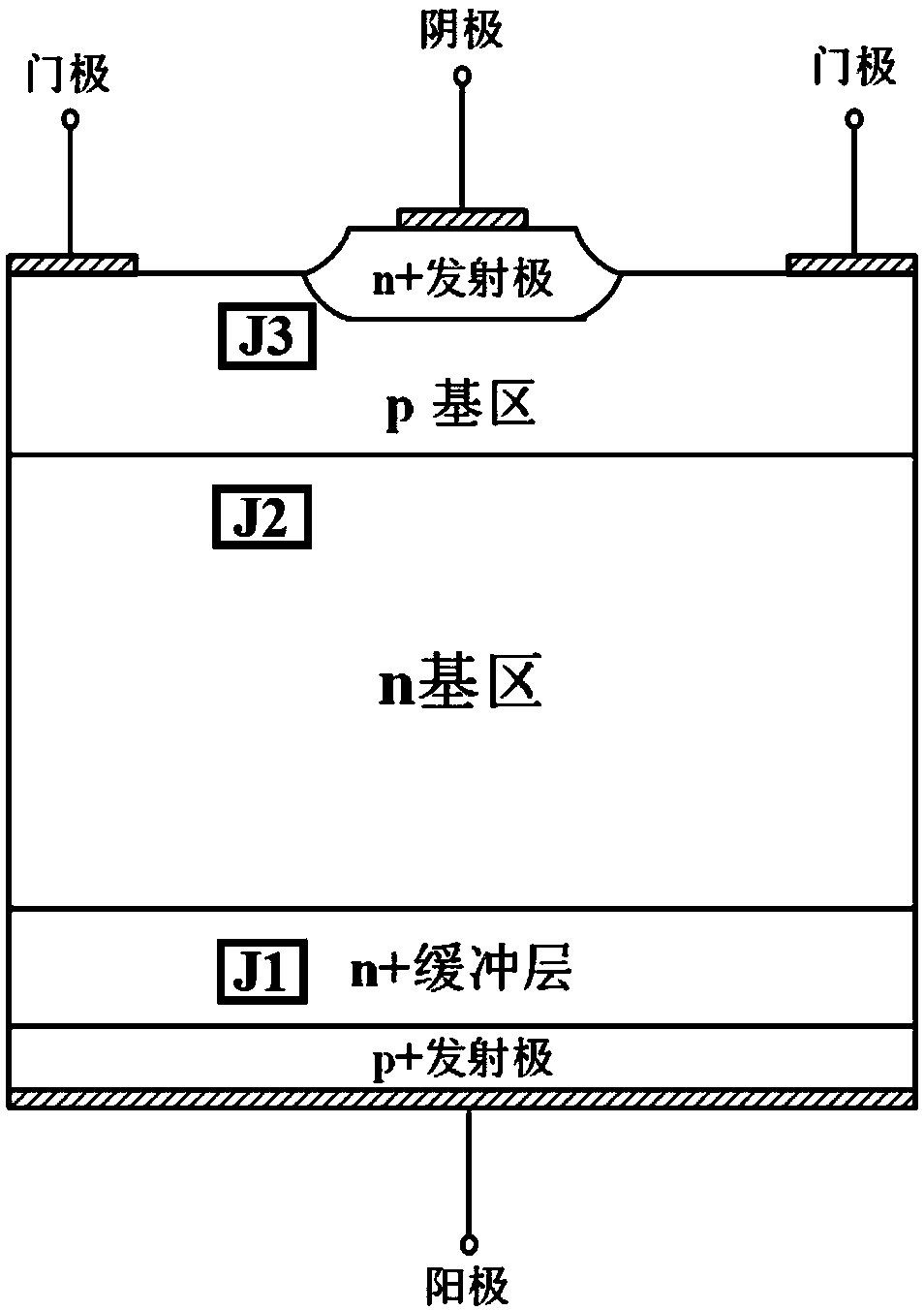
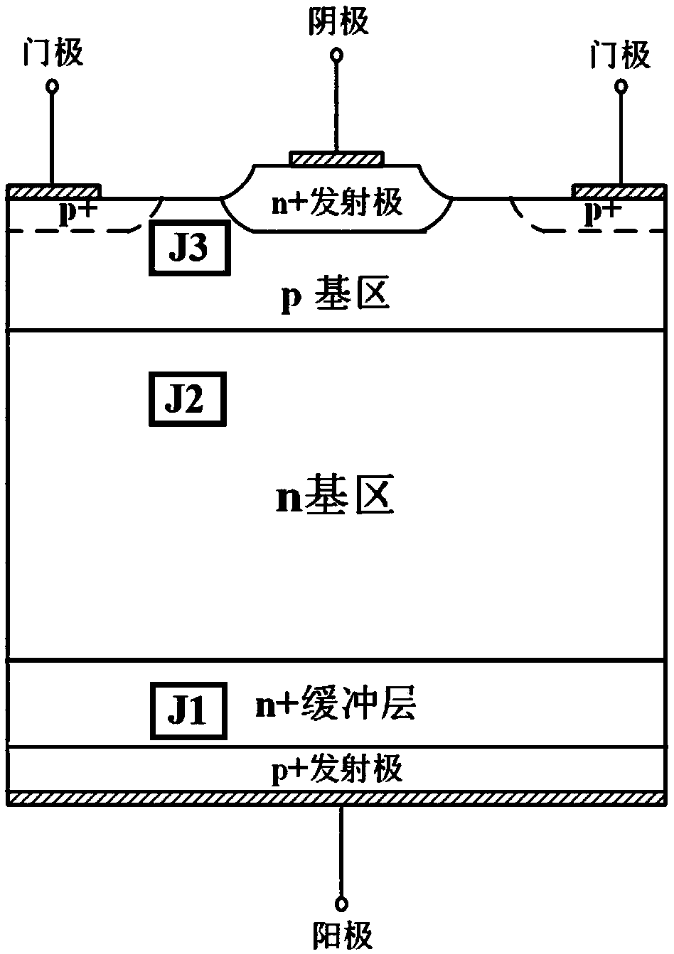
[0029] An embodiment of the present invention provides a device with reverse flow capability, and the device includes a GCT chip module and a driving circuit module. The GCT chip module has a p + emitter, n + buffer layer, n base, p base, n + The emitter constitutes a five-layer thyristor structure, with the p + the anode ...


PUM


Abstract

The invention provides a device having a reverse current-passing function. The device improves the characteristics of a GCT chip by doping an n+ buffer layer and a p+ emitter of a GCT chip module andmaking high concentration p+ doping under a gate pole; by arraging an IGCT driving circuit or an ETO driving circuit connected to the GCT chip module, a reverse passing current is formed between a cathode and the gate pole of the GCT chip, the reverse current-passing function of the IGCT or ETO device is achieved, and it is ensured that the device still has the performances of a conventional IGCTor ETO device in forward conduction; at the same time, the device achieves the inverse current passing of the IGCT or ETO device without change of an original GCT structure and influence on the normalfunctions of the IGCT or ETO device, the process steps are simple, and the yield of industrial production is improved.

Description

technical field [0001] The invention relates to the technical field of power electronics, in particular to a device with reverse flow function. Background technique [0002] figure 1 A schematic diagram of the structure of the traditional GCT unit is shown. As shown in the figure, the existing traditional GCT unit mainly includes two parts: the GCT chip and the corresponding compact gate driver. The inside of the GCT chip is a typical asymmetric structure, and the GCT chip has a PN The PN junction adopts different doping processes, and through diffusion, the P-type semiconductor and the N-type semiconductor are fabricated on the same semiconductor substrate. The semiconductor substrate is usually silicon or germanium. In the P-type The interface between semiconductor and N-type semiconductor forms a space charge region called PN junction, such as figure 2 A schematic structural diagram of the PN junction according to the prior art is shown. The PN junction has unidirecti...

Claims


Application Information

Patent Timeline
Patent Type & Authority Applications(China)
IPC IPC(8): H01L29/06H01L29/08H01L29/747
CPCH01L29/0684H01L29/0834H01L29/747H01L29/744H01L29/42308H01L29/1016H01L29/102
Inventor 刘佳鹏曾嵘周文鹏赵彪余占清陈政宇
Owner TSINGHUA UNIV
Why Eureka
Try Eureka