Drive substrate and display device

A technology for driving substrates and display devices, applied in the field of driving substrates and display devices, can solve problems such as high power loss, increased parasitic capacitance, and high current intolerance, so as to improve signal delay and high power consumption, and minimize parasitic capacitance Effect

Active Publication Date: 2021-09-07
E INK HLDG INC
View PDF16 Cites 0 Cited by
  • Summary
  • Abstract
  • Description
  • Claims
  • Application Information

AI Technical Summary

Problems solved by technology

[0003] However, although oxide semiconductor thin film transistors have good high-voltage resistance characteristics, they are not resistant to high current (high heat). As a result, under high-voltage operating environments, oxide semiconductor thin film transistors cannot withstand high current and cause damage, which in turn makes the display Device not working properly
Therefore, at present, the length of the channel layer of the oxide semiconductor thin film transistor is mostly extended to reduce the current load. However, this method is accompanied by an increase in parasitic capacitance, resulting in serious signal delay and high power loss.

Method used


Image

  • Drive substrate and display device
  • Drive substrate and display device
  • Drive substrate and display device

Examples


Embodiment Construction

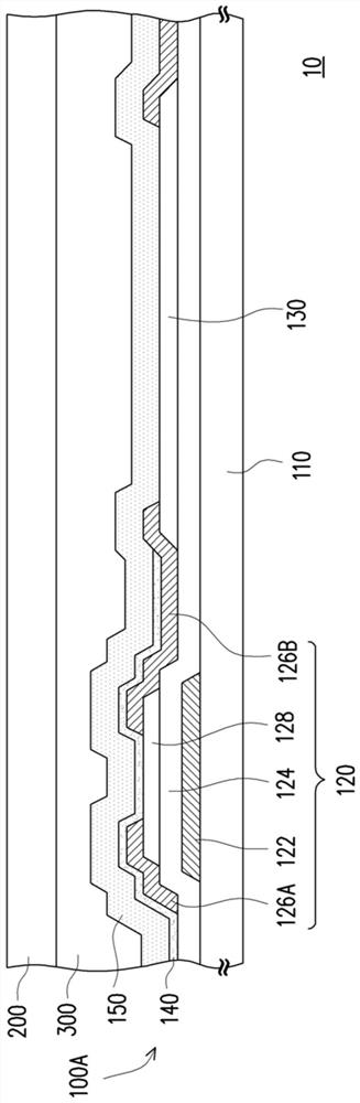
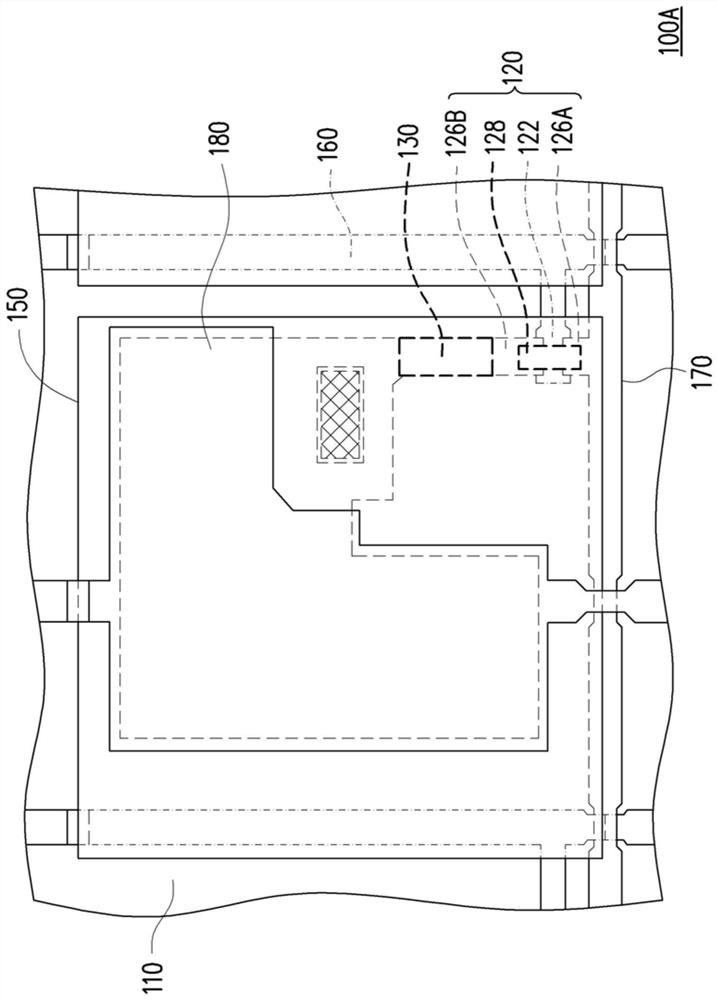
[0046] Figure 1A A schematic partial cross-sectional view of a display device according to an embodiment of the present invention is shown. Figure 1B shown as Figure 1A The schematic top view of the driving substrate. Please refer to Figure 1A , the display device 10 of this embodiment includes a driving substrate 100A and a display medium 200 , wherein the display medium 200 is disposed on the driving substrate 100A. Here, the display medium 200 is, for example, an electrophoretic display film or an electrowetting display film, but is not limited thereto. Such as Figure 1A As shown, the display device 10 of this embodiment may further include a planarization layer 300 disposed between the driving substrate 100A and the display medium 200 for planarizing the driving substrate 100A.

[0047] For details, please also refer to Figure 1A and Figure 1B , the driving substrate 100A of the display device 10 of this embodiment includes a substrate 110, at least one active ele...


PUM


Abstract

The invention provides a driving substrate and a display device. The driving substrate includes a substrate, at least one active element, a resistor, a first protection layer and a second protection layer. The active element with the oxide semiconductor layer and the resistor coupled to the active element are disposed on the substrate. The first protection layer covers the active device, wherein a part of the first protection layer directly contacts the oxide semiconductor layer so that the oxide semiconductor layer has a first conductivity. The second protection layer covers the first protection layer and the resistor, wherein a part of the second protection layer directly contacts the resistor so that the resistor has a second conductivity. The first conductivity is different from the second conductivity.

Description

technical field [0001] The present invention relates to a substrate and an electronic device, in particular to a driving substrate and a display device having the driving substrate. Background technique [0002] In general, amorphous silicon thin film transistors are prone to threshold voltage shift and high leakage current (off current) in high-voltage operating environments, and the molecular structure of amorphous silicon has no order and direction, which will make non-crystalline silicon thin film transistors The movement of electrons in the channel layer of the crystalline silicon thin film transistor is affected, thereby reducing the mobility of carriers. In contrast, the oxide semiconductor thin film transistor has excellent high voltage resistance stability and good carrier mobility. Therefore, the oxide semiconductor thin film transistor has the potential to be a driving element of a display device under a high-voltage operating environment. [0003] However, alth...

Claims


Application Information

Patent Timeline
Patent Type & Authority Patents(China)
IPC IPC(8): H01L27/12G02B26/00G02F1/167G02F1/1675
CPCG02B26/005G02F1/167H01L27/1214
Inventor 陈蔚宗林柏辛蔡学宏
Owner E INK HLDG INC
Why Eureka
Try Eureka