Chip package structure and method for forming same

A chip packaging structure and wafer technology, applied in electrical components, electrical solid devices, circuits, etc., can solve the problems affecting the performance of the packaging structure, reducing the size of semiconductor packaging, wafer peeling, etc., to improve packaging performance, improve warpage and Delamination phenomenon, the effect of reducing the thermal expansion coefficient

Inactive Publication Date: 2019-05-03
SEMICON MFG INT (SHANGHAI) CORP +1
View PDF4 Cites 5 Cited by
  • Summary
  • Abstract
  • Description
  • Claims
  • Application Information

AI Technical Summary

Problems solved by technology

CoW packaging technology has many advantages, such as the ability to achieve high integration of semiconductor devices, reduce the size of semiconductor packages, reduce the cost of final products, simplify assembly processes, and improve yields. After the wafer level molding (wafer level molding) step is completed, the problem of wafer warpage (wafer warpage) is often encountered, which easily leads to the peeling of the stacked wafers from the component wafer, which seriously affects the subsequent packaging processing steps and the final packaging structure. performance

Method used


Image

  • Chip package structure and method for forming same
  • Chip package structure and method for forming same
  • Chip package structure and method for forming same

Examples


Embodiment Construction

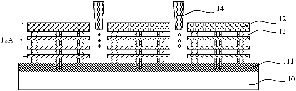
[0031] A manufacturing process flow of a CoW package structure includes the following steps:

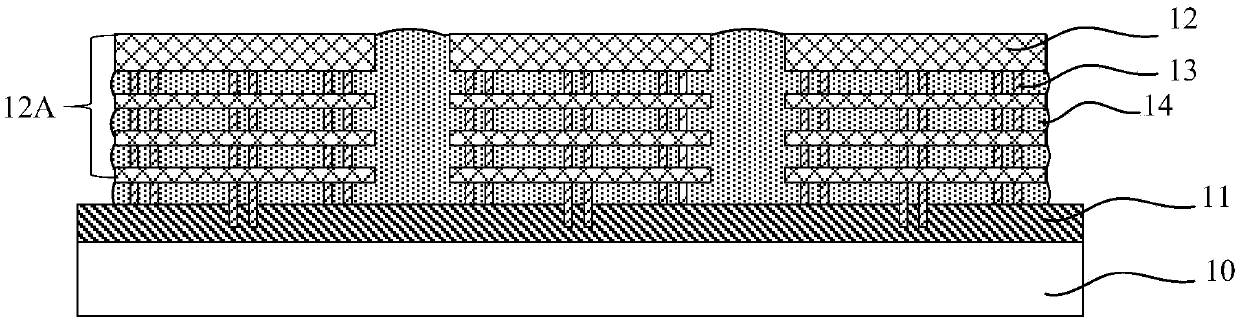
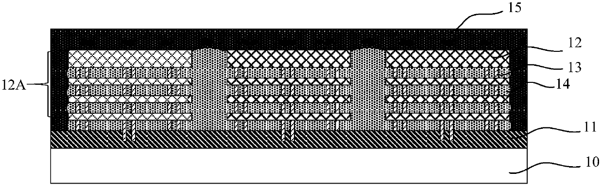
[0032] First, please refer to Figure 1A , paste a carrier 10 on the bottom of the element wafer 11 to support the element wafer 11;

[0033] Then, please continue to refer to Figure 1A stacking (Stacking) a plurality of chips (Die) 12 at corresponding positions on the surface of the component wafer 11, and completing the electrical interconnection between the chips 12 and between the chips and the component wafer 11 by means of reflow or thermocompression bonding, The TSVs (through silicon vias, used for vertical interconnection and conduction) 13 of two adjacent layers of wafers 12 are aligned and electrically contacted to form a plurality of wafer stacks 12A, Figure 1A It is shown that four wafers 12 are stacked into a chip stack 12A, but the actual number of wafers in each wafer stack is not limited to four, and the wafer 12 can be a memory chip such as DRAM or NAND, or a log...


PUM


Abstract

The invention provides a chip package structure and a method for forming the same. By replacing all or a part of primer in a gap between two adjacent wafer stacks with a molding layer having a low thermal expansion coefficient, the amount of the primer is reduced and the thermal expansion coefficient of a packaging colloid composed of the molding layer and the primer is reduced, thereby reducing the CTE mismatch difference between the packaging colloid and the wafer stack and between the packaging colloid and a substrate, improving the warpage and the stratification of the substrate and the wafer stack, and improving packaging performance.

Description

technical field [0001] The invention relates to the technical field of integrated circuit manufacturing, in particular to a chip packaging structure and a forming method thereof. Background technique [0002] Chip on wafer (CoW) packaging technology, as one of the advanced packaging (Package) technologies, can stack multiple chips separately on the positions of good chips that are pre-identified on a device wafer (Device Wafer) (Die, that is, a block with complete functions cut out from the wafer) to meet different functions, and then realize the manufacture of three-dimensional semiconductor integrated circuit (IC) products. CoW packaging technology has many advantages, such as the ability to achieve high integration of semiconductor devices, reduce the size of semiconductor packages, reduce the cost of final products, simplify assembly processes, and improve yields. After the wafer level molding (wafer level molding) step is completed, the problem of wafer warpage (wafer ...

Claims


Application Information

Patent Timeline
Patent Type & Authority Applications(China)
IPC IPC(8): H01L25/065H01L23/31H01L23/29H01L21/56
Inventor 陈彧
Owner SEMICON MFG INT (SHANGHAI) CORP
Why Eureka
Try Eureka