
Cross blind pixel detection and correction device and method for InGaAs short wave infrared imager

A short-wave infrared and correction device technology, applied in measurement devices, radiation pyrometry, instruments, etc., can solve the problems of inapplicability, the compensation effect is difficult to achieve expectations, and the image quality cannot be obtained, and achieves small temperature influence and good processing effect. , the effect of uniform light

Active Publication Date: 2019-05-10
SHANDONG UNIV
View PDF12 Cites 10 Cited by
  • Summary
  • Abstract
  • Description
  • Claims
  • Application Information

AI Technical Summary

Problems solved by technology

However, these methods are inapplicable when dealing with cross-blind pixels, and the compensation effect is difficult to meet expectations, and sometimes even aggravates the inhomogeneity of the image
Therefore, if the focal plane detector used in the SWIR imager has blind cross pixels, the existing processing methods will not be able to obtain the best image quality

Method used


Image

  • Cross blind pixel detection and correction device and method for InGaAs short wave infrared imager
  • Cross blind pixel detection and correction device and method for InGaAs short wave infrared imager
  • Cross blind pixel detection and correction device and method for InGaAs short wave infrared imager

Examples


Embodiment Construction

[0032] The following will clearly and completely describe the technical solutions in the embodiments of the present invention with reference to the accompanying drawings in the embodiments of the present invention. Obviously, the described embodiments are only some, not all, embodiments of the present invention. Based on the embodiments of the present invention, all other embodiments obtained by persons of ordinary skill in the art without creative efforts fall within the protection scope of the present invention.

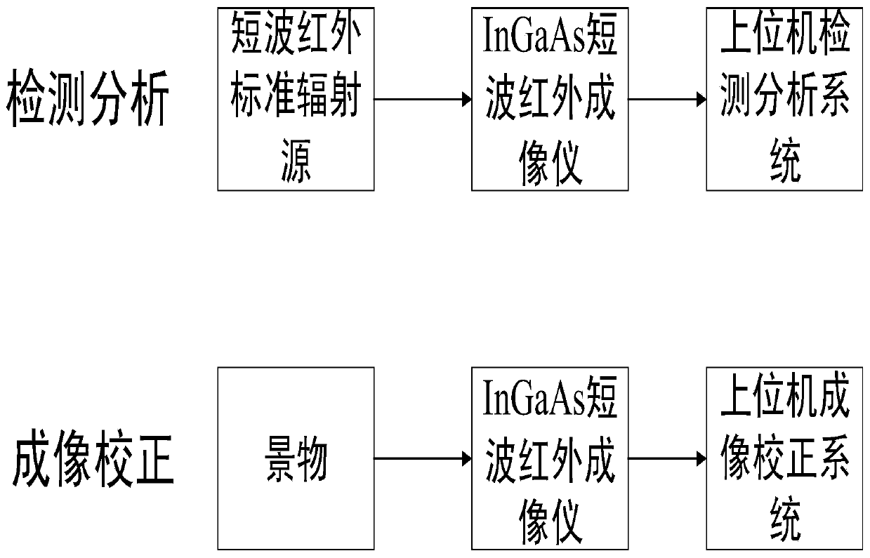
[0033] The present invention first claims protection of a cross-blind element detection and correction device for an InGaAs short-wave infrared imager, which is characterized in that it includes:

[0034] Shortwave infrared standard radiation source, InGaAs shortwave infrared imager, host computer detection and analysis system and host computer imaging correction system;

[0035] The short-wave infrared standard radiation source is used as a correction light source...


PUM


Abstract

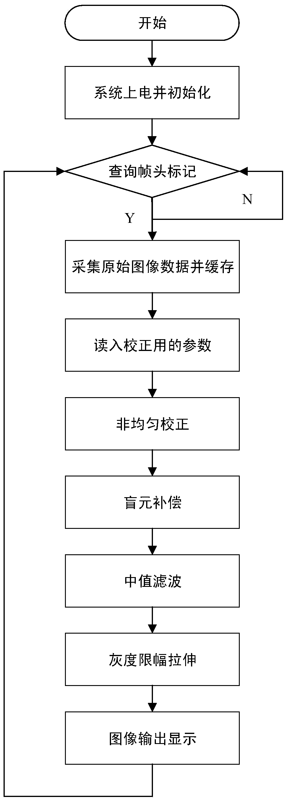
The invention discloses a cross blind pixel detection and correction device and methodfor a InGaAs short wave infrared imager. The device comprises a short wave infrared standard radiation source, theInGaAs short wave infrared imager, an upper computer detection analysis system and an upper computer imaging correction system. The upper computer detection analysis system collects correction imagedata uploaded to an upper computer. The upper computer imaging correction system collects original image data uploaded to the upper computer. According to the method provided by the invention, detection and processing aremainly carried out for cross blind pixels. Compared with a conventional correction processing method, the method has the advantage that a processing effect for the cross blind pixels is better. After the InGaAs short wave infrared imager carries out one-time correction parameter operation, images can be corrected through call of parameters each time when imaging is carried out, and the correction parameters do not need to be computed again. For the feature that the InGaAs short wave infrared imager carries out the imaging through utilization of scenery reflected light, anintegrating sphere is employed as the short wave infrared standard radiation source, light emergence is relatively uniform, and the temperature influence is relatively low.

Description

technical field [0001] The invention belongs to the field of short-wave infrared image processing, and more specifically relates to a cross blind element detection and correction device and method of an InGaAs short-wave infrared imager. Background technique [0002] In recent years, with the rapid development of InGaAs material growth technology and its focal plane preparation technology, a short-wave infrared focal plane detector based on InGaAs material appeared and matured rapidly, driving the progress of short-wave infrared solid-state imaging technology. InGaAs is a pseudo-binary semiconductor material of the III-V group. It has a zinc blende cubic crystal structure. By adjusting the components of In and Ga, its corresponding wavelength range can reach 0.5μm-2.5μm, and it has a high quantum efficiency and sensitivity. The short-wave infrared focal plane detector based on InGaAs material has the advantages of uncooled room temperature operation, high detection rate, an...

Claims


Application Information

Patent Timeline
Patent Type & Authority Applications(China)
IPC IPC(8): G01J5/00
Inventor 李永富费宬刘俊良郭进康佳龙
Owner SHANDONG UNIV
Learn More