
Low-temperature microwave annealing method for improving optical-electrical characteristic of silicon superlattice film

A technology of microwave annealing and photoelectric characteristics, applied in the direction of circuits, electrical components, semiconductor devices, etc., can solve problems such as high temperature and damage to silicon superlattice structure, and achieve high yield, low annealing temperature, and strong repeatability Effect

Active Publication Date: 2019-05-10
FUDAN UNIV
View PDF4 Cites 2 Cited by
  • Summary
  • Abstract
  • Description
  • Claims
  • Application Information

AI Technical Summary

Problems solved by technology

[0004] The purpose of the present invention is to overcome the high temperature and easy thermal diffusion in the traditional silicon superlattice thin film annealing technology and destroy the present situation of silicon superlattice structure, propose a kind of Low-temperature microwave annealing method for improving photoelectric properties of silicon superlattice thin films

Method used


Image

  • Low-temperature microwave annealing method for improving optical-electrical characteristic of silicon superlattice film
  • Low-temperature microwave annealing method for improving optical-electrical characteristic of silicon superlattice film
  • Low-temperature microwave annealing method for improving optical-electrical characteristic of silicon superlattice film

Examples


Embodiment 1

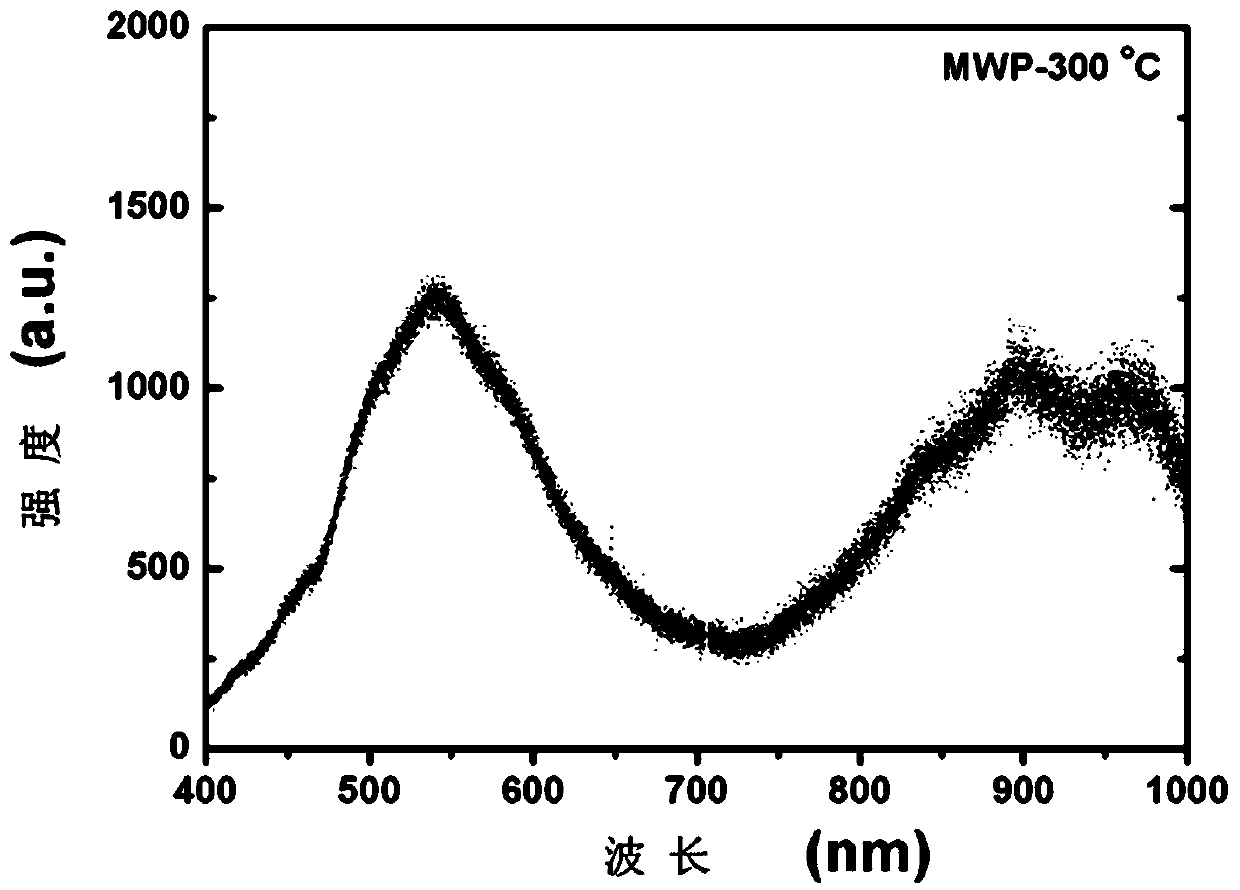
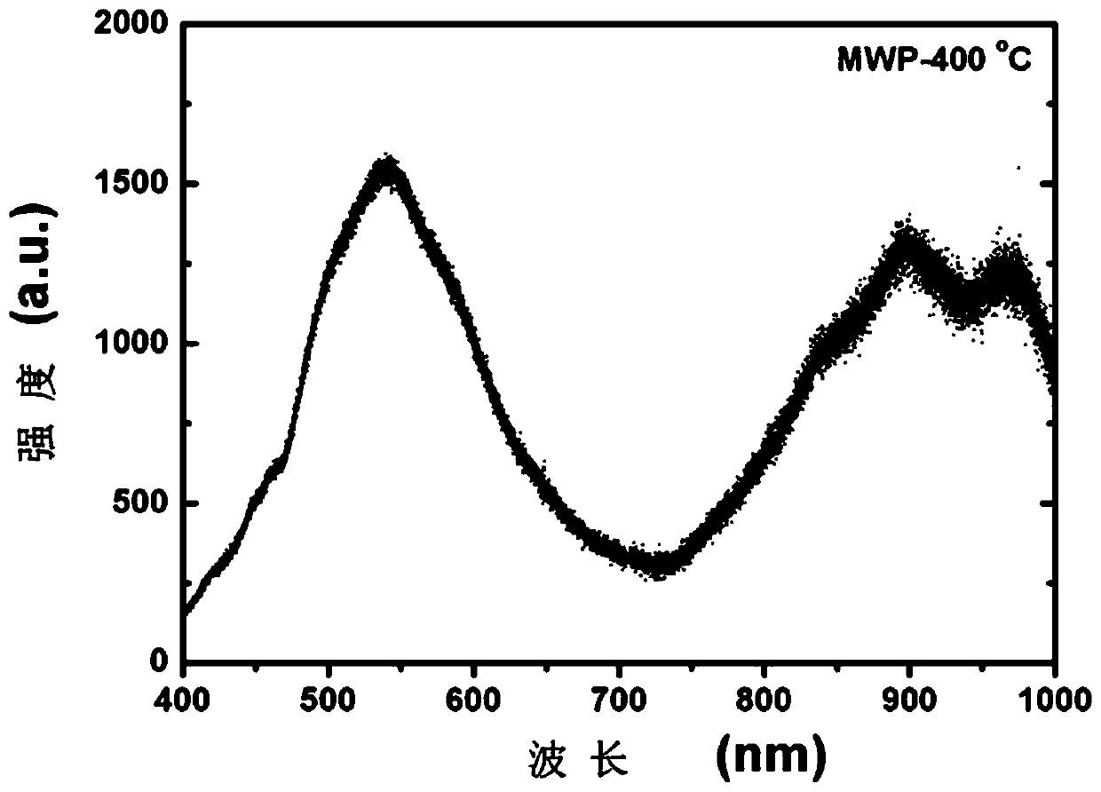
[0027] A method for improving SiO 2 / SiN x Process flow of low-temperature microwave annealing method for photoelectric properties of silicon superlattice thin films (such as figure 1 shown), including the following steps:

[0028] Step 1: RCA standard cleaning process cleans a p-type 4-inch silicon wafer with a thickness of about 250 μm and a crystal orientation of (100) and blows it dry with high-purity nitrogen.

[0029] Step 2, Deposit SiO with a thickness of 105 nm on the Si wafer substrate by ALD technology 2 / SiN x Laminated thin films, where SiN in each lamination cycle x Layer thickness about 2 nm, SiO 2 The layer thickness is about 3 nm, and the total number of lamination cycles is 20.

[0030] Step 3, before annealing, nitrogen gas with a flow rate of 20 sccm was preliminarily passed into the microwave annealing chamber for 20 minutes.

[0031] Step 4, continue to flow into the nitrogen gas with a flow rate of 20 sccm as the annealing atmosphere, and SiO on t...


PUM


Abstract

The invention discloses a low-temperature microwave annealing method for improving the optical-electrical characteristic of a silicon superlattice film. The low-temperature microwave annealing methodcomprises the specific steps that 1, before annealing, inertia gas is introduced into a microwave annealing cavity in advance, so that a pure inertia atmosphere is formed in the cavity; 2, the inertiagas continues being introduced to serve as an annealing atmosphere, the silicon superlattice film is put into the middle of the microwave annealing cavity, the annealing power and the maximum temperature in the annealing process are set, the annealing time with the corresponding duration is set, and microwave annealing is started, wherein the maximum temperature in the annealing process is 300-500 DEG C; and 3, after microwave annealing and after natural cooling of the temperature in the cavity, the modified and optimized silicon superlattice film is obtained. The low-temperature microwave annealing method is high in reliability and repeatability, the finished product rate of the modified and optimized silicon superlattice film prepared through the low-temperature microwave annealing method is high, and the method with guiding significance is provided for low-temperature annealing of the silicon superlattice film.

Description

technical field [0001] The invention relates to the technical fields of microwave annealing technology and silicon superlattice thin film preparation, in particular to a low-temperature microwave annealing method for improving the photoelectric properties of silicon superlattice thin film. Background technique [0002] In recent years, with the vigorous development of integrated circuits, silicon-based light-emitting devices have increasingly become the key to the development of optoelectronic integration and have received extensive research attention. Among many silicon-based materials, silicon-based superlattice structures, such as Si / SiGe, Si / SiC, Si / Ge, Si / SiO 2 , SiO x / SiO 2 、SiN x / SiO 2 Such superlattice thin films are one of the excellent materials for building high-efficiency silicon-based light-emitting devices and manufacturing silicon photoelectric integrated circuits, and have great potential for application and development. [0003] The process of transfo...

Claims


Application Information

Patent Timeline
IPC IPC(8): H01L21/02H01L33/00
CPCY02P70/50
Inventor 卢红亮朱立远马宏平张卫
Owner FUDAN UNIV
Learn More