Color-variable flexible electronic skin and preparation method thereof
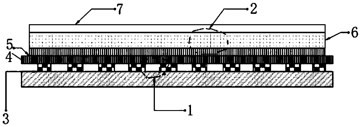
An electronic skin and flexible technology, applied in the field of color-changing flexible electronic skin and its preparation, can solve the problems of high cost and complicated electronic skin process, and achieve the effect of low cost, obvious resistance change and simple structure
- Summary
- Abstract
- Description
- Claims
- Application Information
AI Technical Summary
Problems solved by technology
Method used
Image
Examples
Embodiment 1
[0031] A preparation of a color-changing flexible electronic skin mainly includes the following steps:
[0032] Step 1. Preparation of polydimethylsiloxane (PDMS) substrate: PDMS and curing agent were mixed in a ratio of 10:1 and stirred for 5 minutes, then the mixture was placed in a vacuum drying oven to exhaust and dry until no visible Pour the PDMS mixture into a plastic box with a diameter of 10 cm, put it on a heating plate and cure it at a temperature of 65 ° C for 7 hours to prepare a PDMS substrate with uniform thickness.
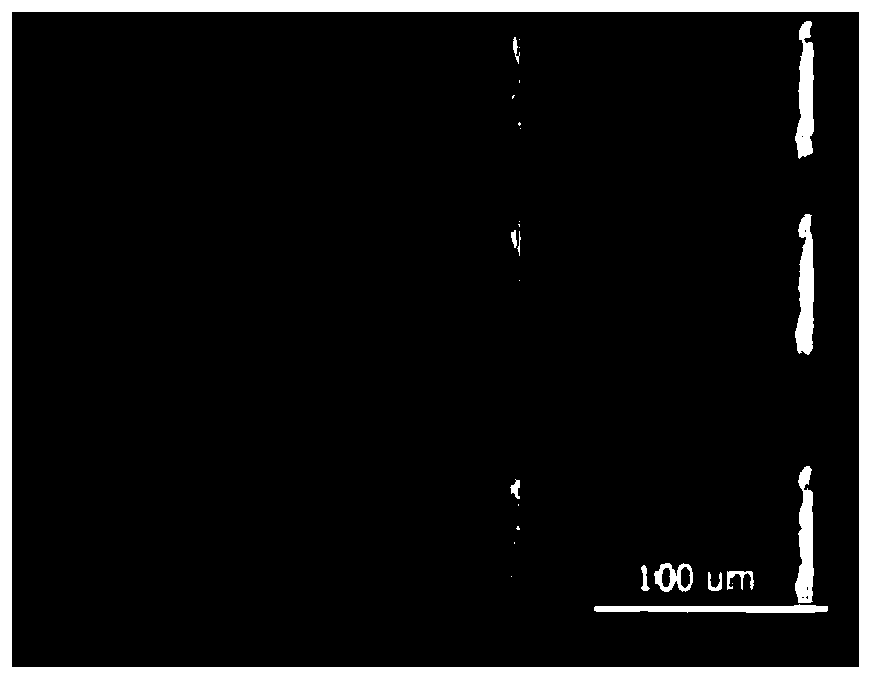
[0033] Step 2, preparation of bump microstructure PDMS: make a silicon mold with many regular pit arrays by plasma etching, the mold is as follows figure 2 As shown; PDMS and curing agent were mixed in a ratio of 10:1 and stirred for 5 minutes, then the mixture was placed in a vacuum drying oven to ventilate and dry until no bubbles were seen, and the PDMS mixture was poured into a silicon template and placed in a heated The board was cured at a ...
Embodiment 2
[0041] Step 1. Preparation of polydimethylsiloxane (PDMS) substrate: PDMS and curing agent were mixed in a ratio of 10:1 and stirred for 2 minutes, then the mixture was placed in a vacuum drying oven to exhaust and dry until no visible Pour the PDMS mixture into a plastic box with a diameter of 10 cm, put it on a heating plate and cure it at a temperature of 65 ° C for 7 hours to prepare a PDMS substrate with uniform thickness.
[0042] Step 2. Preparation of bump microstructure PDMS: use plasma etching to make a silicon mold with many regular pit arrays; mix PDMS and curing agent at a ratio of 10:1 and stir for 2 minutes, then place the mixture in a vacuum to dry Air and dry in the box until no bubbles can be seen, pour the PDMS mixture into the silicon template, put it on a heating plate and cure it at 65°C for 7 hours, and prepare a PDMS substrate with a bump microstructure with uniform thickness.
[0043] Step 3, preparation of the single-walled carbon nanotube film: the P...
Embodiment 3
[0050] Step 1. Preparation of polydimethylsiloxane (PDMS) substrate: PDMS and curing agent were mixed in a ratio of 10:1 and stirred for 3 minutes, then the mixture was placed in a vacuum drying oven to exhaust and dry until no visible Pour the PDMS mixture into a plastic box with a diameter of 10 cm, put it on a heating plate and cure it at a temperature of 65 ° C for 7 hours to prepare a PDMS substrate with uniform thickness.
[0051] Step 2. Preparation of bump microstructure PDMS: use plasma etching to make a silicon mold with many regular pit arrays; mix PDMS and curing agent at a ratio of 10:1 and stir for 5 minutes, then place the mixture in a vacuum to dry Air and dry in the box until no bubbles can be seen, pour the PDMS mixture into the silicon template, put it on a heating plate and cure it at 65°C for 7 hours, and prepare a PDMS substrate with a bump microstructure with uniform thickness.
[0052] Step 3, preparation of the multi-walled carbon nanotube film: the PD...
PUM
 Abstract
Description
Claims
Application Information
 - R&D
- Intellectual Property
- Life Sciences
- Materials
- Tech Scout
- Unparalleled Data Quality
- Higher Quality Content
- 60% Fewer Hallucinations
Browse by: Latest US Patents, China's latest patents, Technical Efficacy Thesaurus, Application Domain, Technology Topic, Popular Technical Reports.
© 2025 PatSnap. All rights reserved.Legal|Privacy policy|Modern Slavery Act Transparency Statement|Sitemap|About US| Contact US: help@patsnap.com


