OLED screen body used for fingerprint recognition device as well as fingerprint recognition device
A technology for fingerprint identification and encapsulation of cover plates, applied in character and pattern recognition, electric solid-state devices, semiconductor devices, etc., can solve the problem of low signal-to-noise ratio of fingerprint identification detection structure, unable to achieve full-plane fingerprint identification, and affecting fingerprint detection. Signal detection and other problems, to achieve the effect of improving recognition sensitivity, improving recognition sensitivity, and preventing interference
- Summary
- Abstract
- Description
- Claims
- Application Information
AI Technical Summary
Problems solved by technology
Method used
Image
Examples
Embodiment 1
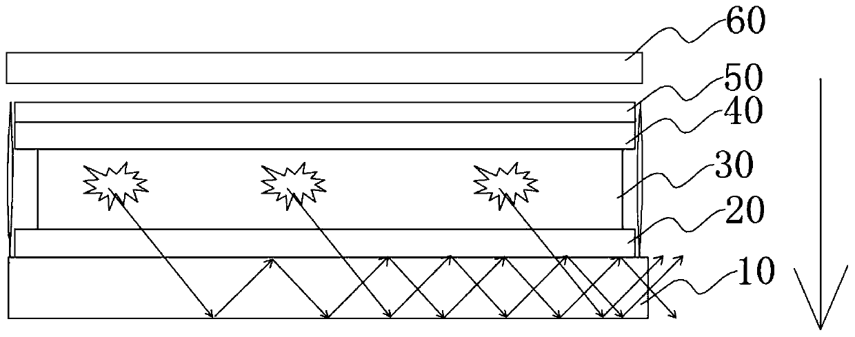
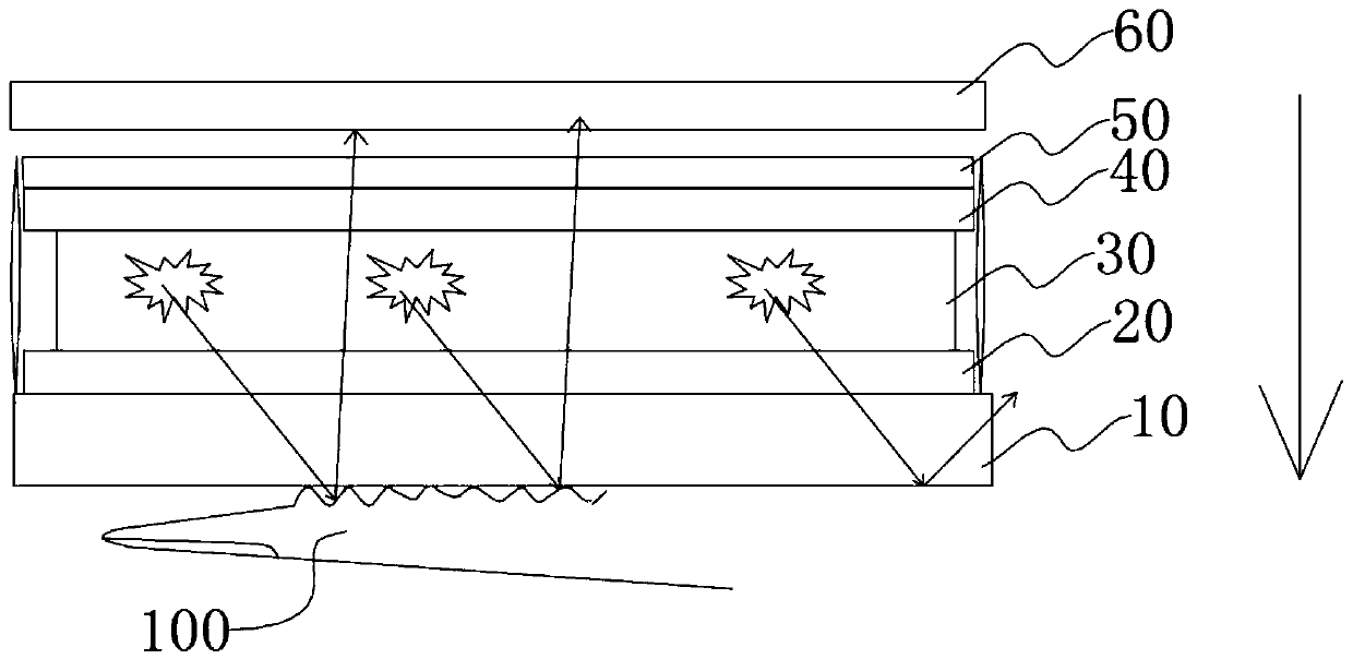
[0059] For example figure 1 and figure 2 As shown, the OLED fingerprint identification device includes from bottom to top: a substrate 10, a first electrode 20, an organic functional layer 30, a second electrode 40, a package cover 50 and a receiver 60; the direction of the arrow in the figure is the direction of light output, The light-emitting surface of the OLED fingerprint recognition device in this embodiment is set on the bottom surface, and it is a bottom-surface light-emitting fingerprint recognition device. Therefore, the second electrode 40 in this embodiment is a reflective electrode, and the first electrode 20 is a basic electrode.
[0060] Such as figure 1 As shown, in the state of the bare screen, most of the light is sealed in the substrate 10, and only a small amount of light leaks from the side of the substrate 10; figure 2 As shown, after the finger 100 is covered, the finger 100 changes the light emitting direction, so that a large amount of light is ref...
Embodiment 2
[0116] For example Figure 4 As shown, the OLED fingerprint identification device includes from bottom to top: a receiver 60, a substrate 10, a first electrode 20, an organic functional layer 30, a second electrode 40, and a packaging cover 50; the direction of the arrow in the figure is the direction of light output, The light-emitting surface of the OLED fingerprint recognition device in this embodiment is set on the top surface, and it is a top-surface light-emitting fingerprint recognition device. Therefore, the first electrode 20 in this embodiment is a reflective electrode, and the second electrode 40 is a basic electrode.
[0117] In this embodiment, the first electrode 20 is a metal cathode made of Al (aluminum) with a thickness of 150 nm;
[0118] The organic functional layer includes from bottom to top:
[0119] Electron injection layer: main material LiF (lithium fluoride), thickness 0.8nm;
[0120] Electron transport layer: main material Bphen (4,7-diphenyl-1,10-...
Embodiment 3
[0132] Embodiment 3: On the basis of Embodiment 2, the thickness of the electron transport layer is changed to 57.2 nm; therefore, the distance H from the reflective electrode to the light-emitting layer is 58 nm.
[0133] Control group 2: OLED fingerprint identification device includes from bottom to top: receiver 60, substrate 10, first electrode 20, organic functional layer 30, second electrode 40, packaging cover 50; OLED fingerprint identification device in this embodiment The light-emitting surface is set on the top surface, which is a top-surface light-emitting fingerprint recognition device. Therefore, the first electrode 20 in the second comparison group is a reflective electrode, and the second electrode 40 is a basic electrode.
[0134] In the second control group, the first electrode 20 is a metal cathode made of Al with a thickness of 150nm; the organic functional layer includes from bottom to top:
[0135] Electron injection layer: main material LiF (lithium fluo...
PUM
| Property | Measurement | Unit |
|---|---|---|
| Thickness | aaaaa | aaaaa |
| Thickness | aaaaa | aaaaa |
| Thickness | aaaaa | aaaaa |
Abstract
Description
Claims
Application Information


