Bispectral metasurface integrated uncooled infrared detector and manufacturing method
An uncooled infrared and metasurface technology, applied in electrical radiation detectors and other directions, can solve the problems of reduced performance, increased equivalent heat capacity, increased thickness of the absorption layer, etc., to improve performance, achieve equivalent noise temperature difference, Process compatible effects
- Summary
- Abstract
- Description
- Claims
- Application Information
AI Technical Summary
Problems solved by technology
Method used
Image
Examples
Embodiment 1
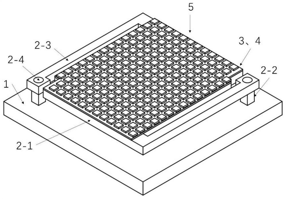
[0049] Bispectral metasurface integrated uncooled infrared detectors such as figure 1 shown. The focal plane pixel unit metal microarray structure is as follows Figure 4 As shown, the first dielectric layer 5-2-1 is made of germanium (Ge), the metal microarray 5-3 is made of gold (Au), each metal unit is a cross-shaped sub-wavelength super-pixel, and two adjacent metal The structure of the unit is different. The side length of the cross-shaped subwavelength structure 5-3-1 of the two structures is 1 micron, and the line widths are 1 micron and 0.3 micron, respectively. Infrared radiation with wavelengths near 5 microns and 9 microns is captured by the bispectral absorbing film layer 5, and converts light energy into Joule heat of the metal structure and phonon absorption of the dielectric structure, thereby heating the thermistor layer 3 , thereby converting the temperature change of the dual-band absorbing film layer 5 caused by the measured infrared radiation signal into...
Embodiment 2
[0061] Bispectral metasurface integrated uncooled infrared detectors such as figure 1 shown. The focal plane pixel unit metal microarray structure is as follows Figure 5 As shown, the second dielectric layer 5-2-2 is made of silicon (Si), the metal microarray 5-3 is made of gold (Au), and each metal unit is a square ring two-layer nested structure 5-3-2, the square The side length of the ring is 3 microns, the line width is 0.5 microns, the side length of the inner square is 0.8 microns, and the infrared radiation near the wavelength of 3 microns and 9 microns is captured by the bispectrum absorption film layer 5, and the light energy is converted into Joule heat of the metal structure and the phonon absorption of the dielectric structure, and then heat the thermistor layer 3, so that the temperature change of the bispectrum absorbing film layer 5 caused by the measured infrared radiation signal is converted into an electrical signal, and then obtained by the readout circuit...
PUM
| Property | Measurement | Unit |
|---|---|---|
| thickness | aaaaa | aaaaa |
| thickness | aaaaa | aaaaa |
| thickness | aaaaa | aaaaa |
Abstract
Description
Claims
Application Information


