Non-refrigeration infrared focal plane of compound absorption film layer and preparation method thereof
An uncooled infrared, absorbing film technology, applied in electrical radiation detectors and other directions, can solve the problems of reduced performance, increased equivalent heat capacity, increased thickness of the absorbing layer, etc., to achieve performance, increase process complexity, The effect is favorable for large-scale low-cost preparation
- Summary
- Abstract
- Description
- Claims
- Application Information
AI Technical Summary
Problems solved by technology
Method used
Image
Examples
Embodiment 1
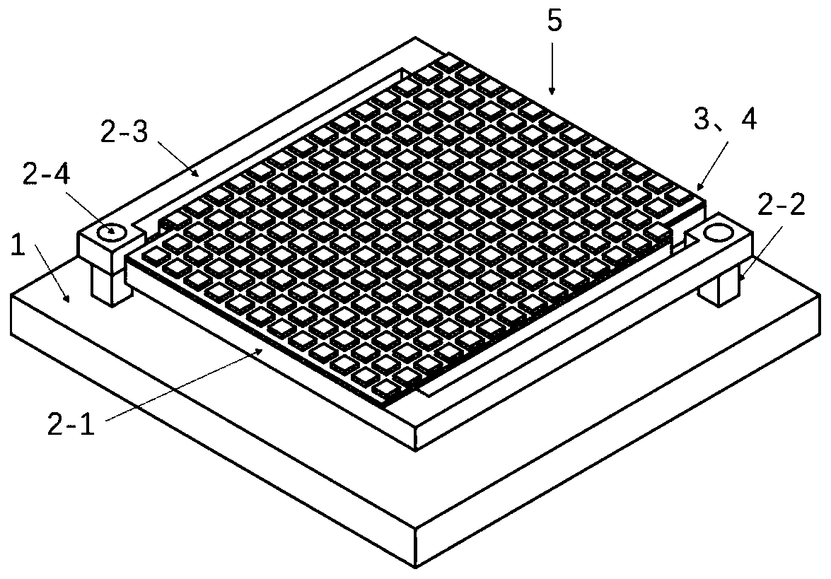
[0050] An uncooled infrared focal plane of a composite absorbing film such as figure 1 shown. The focal plane pixel unit metal microarray structure is as follows Figure 4 As shown, the first dielectric layer 5-2-1 is made of germanium (Ge), the metal microarray 5-3 is made of gold (Au), and each metal unit is a super-pixel with a square structure 5-3-1. The side length of the square structure 5-3-1 is 1 μm. The infrared radiation with a wavelength near 8 microns is captured by the composite absorbing film layer 5, and converts the light energy into Joule heat of the metal structure and phonon absorption of the dielectric structure, and then heats the thermistor layer 3, thereby turning the measured The temperature change of the composite absorbing film layer 5 caused by the infrared radiation signal is converted into an electrical signal, and the infrared information of the target is obtained through the readout circuit 1 to realize infrared detection and imaging.
[0051]...
Embodiment 2
[0062] An uncooled infrared focal plane structure of a composite absorbing film such as figure 1 shown. The focal plane pixel unit metal microarray structure is as follows Figure 5 As shown, the second dielectric layer 5-2-2 is made of silicon (Si), the metal microarray 5-3 is made of gold (Au), each metal unit is a cross-shaped structure 5-3-2, and the length of the long side is 2 microns , the short side length is 1 micron, and the infrared radiation with a wavelength of 9 microns is captured by the composite absorbing film layer 5, and the light energy is converted into Joule heat of the metal structure and phonon absorption of the dielectric structure, and then the thermistor layer 3 is heating, thereby converting the temperature change of the composite absorbing film layer 5 caused by the measured infrared radiation signal into an electrical signal, and then obtaining the infrared information of the target through the readout circuit 1 to realize infrared detection and ...
PUM
 Abstract
Description
Claims
Application Information


