
Semiconductor device and forming method thereof

A semiconductor and device technology, applied in the field of semiconductor devices and their formation, can solve problems such as short circuit between source and drain doped regions and gate structure, leakage, influence of gate dielectric layer, etc., and achieve low etching rate and reduce loss

Active Publication Date: 2019-05-28
SEMICON MFG INT (SHANGHAI) CORP +1
View PDF5 Cites 0 Cited by
  • Summary
  • Abstract
  • Description
  • Claims
  • Application Information

AI Technical Summary

Problems solved by technology

[0004] However, in the prior art, when the source-drain doped region is formed, various processes such as etching and cleaning will affect the gate dielectric layer, and in severe cases, a short circuit will occur between the source-drain doped region and the gate structure. , resulting in leakage

Method used


Image

  • Semiconductor device and forming method thereof
  • Semiconductor device and forming method thereof
  • Semiconductor device and forming method thereof

Examples


Embodiment Construction

[0028] In existing fin field effect transistors, before forming the gate structure, a gate dielectric layer is usually formed on the surface of the fin to protect the fin and avoid leakage between the source-drain doped region and the gate structure. current.

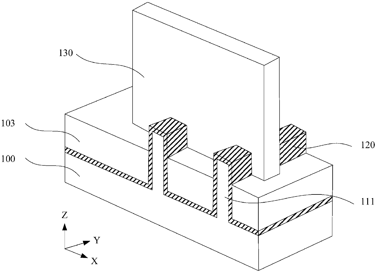
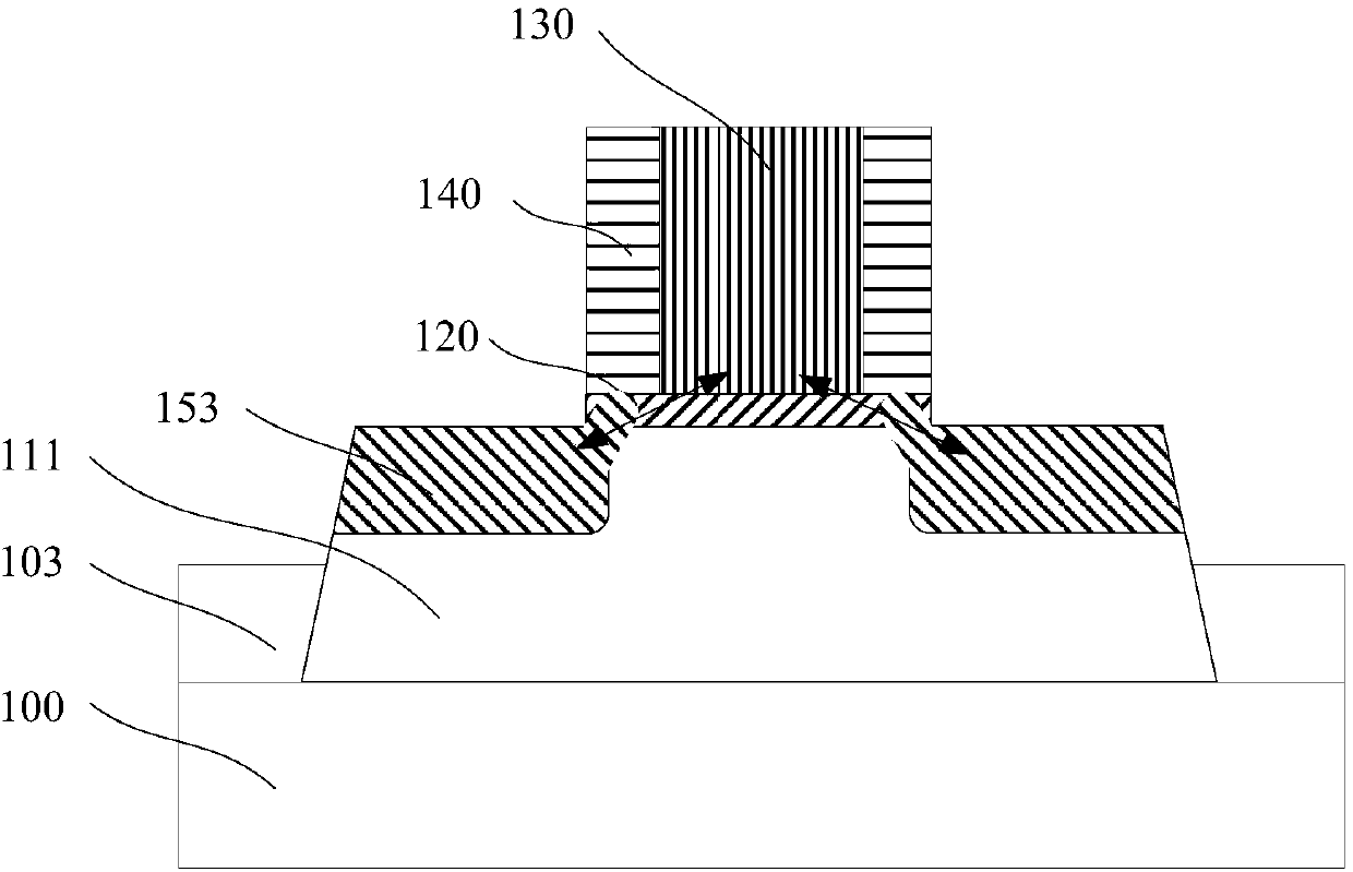
[0029] refer to figure 1 and figure 2 , Figure 1 to Figure 2 It is a structural schematic diagram of a semiconductor device in the prior art. in, figure 1 is a schematic diagram of a three-dimensional structure of a semiconductor device, figure 2 It is a schematic cross-sectional structure diagram of a semiconductor device.

[0030] Combine below Figure 1 to Figure 2 The fin field effect transistor will be described.

[0031] Such as figure 1 The illustrated semiconductor device is a fin field effect transistor, which may include a semiconductor substrate 100 , a fin portion 111 , an isolation layer 103 , a gate dielectric layer 120 and a gate structure 130 .

[0032] Wherein, the fin portion 111 is locate...


PUM


Abstract

The invention discloses a semiconductor device and a forming method thereof, and the method comprises the following steps: providing a semiconductor substrate, and forming protruding fin parts on thesurface of the semiconductor substrate; forming a gate dielectric layer on the surfaces of the fin parts; forming a gate structure crossing the fin parts on the semiconductor substrate; carrying out ion implantation on the gate dielectric layer so as to form doped dielectric layers in the gate dielectric layer at two sides of the gate structure; etching the fin parts on the two sides of the grid electrode structure to form replacement grooves in the fin parts, reserving the doped dielectric layer between the replacement grooves and the grid electrode structure, and enabling the etching rate ofthe etching to the doped dielectric layer to be lower than that of the etching to the grid dielectric layer; and forming a source-drain doped region in the replacement groove. According to the scheme, the source-drain doped region and the gate structure can be effectively separated, and the performance of the semiconductor device is improved.

Description

technical field [0001] The invention relates to the field of semiconductor manufacturing, in particular to a semiconductor device and a forming method thereof. Background technique [0002] Fin Field Effect Transistor (FinFET) is an emerging multi-gate device, which usually includes a fin protruding from the surface of the semiconductor substrate, a gate structure covering part of the top surface and sidewall of the fin, located at the gate Source and drain doped regions in the fins on both sides of the structure. [0003] Specifically, before forming the gate structure, a gate dielectric layer is usually formed on the surface of the fin to protect the fin and prevent leakage current between the source-drain doped region and the gate structure. [0004] However, in the prior art, when the source-drain doped region is formed, various processes such as etching and cleaning will affect the gate dielectric layer, and in severe cases, a short circuit will occur between the sourc...

Claims


Application Information

Patent Timeline
Patent Type & Authority Applications(China)
IPC IPC(8): H01L21/336H01L29/78
Inventor 金兰刘轶群
Owner SEMICON MFG INT (SHANGHAI) CORP
Features
  • Generate Ideas
  • Intellectual Property
  • Life Sciences
  • Materials
  • Tech Scout
  • Unparalleled Data Quality
  • Higher Quality Content
  • 60% Fewer Hallucinations
Learn More