COB camera module and packaging method thereof

A camera module and packaging method technology, applied in radiation control devices and other directions, can solve the problems of photosensitive chip damage, affecting imaging quality, and difficult to remove impurity particles.

Active Publication Date: 2019-05-31
SHENZHEN AOLAN TECH CO LTD
View PDF10 Cites 2 Cited by
  • Summary
  • Abstract
  • Description
  • Claims
  • Application Information

AI Technical Summary

Problems solved by technology

However, in the COB camera module, since there is no glass cover protection, foreign particles such as dust will directly adhere to the photosensitive chip, and particles larger than 1 pixel can cause black shadows on the image, and foreign particles are not easy to remove
In the traditional method, in ord

Method used


Image

  • COB camera module and packaging method thereof
  • COB camera module and packaging method thereof
  • COB camera module and packaging method thereof

Examples


Embodiment 1

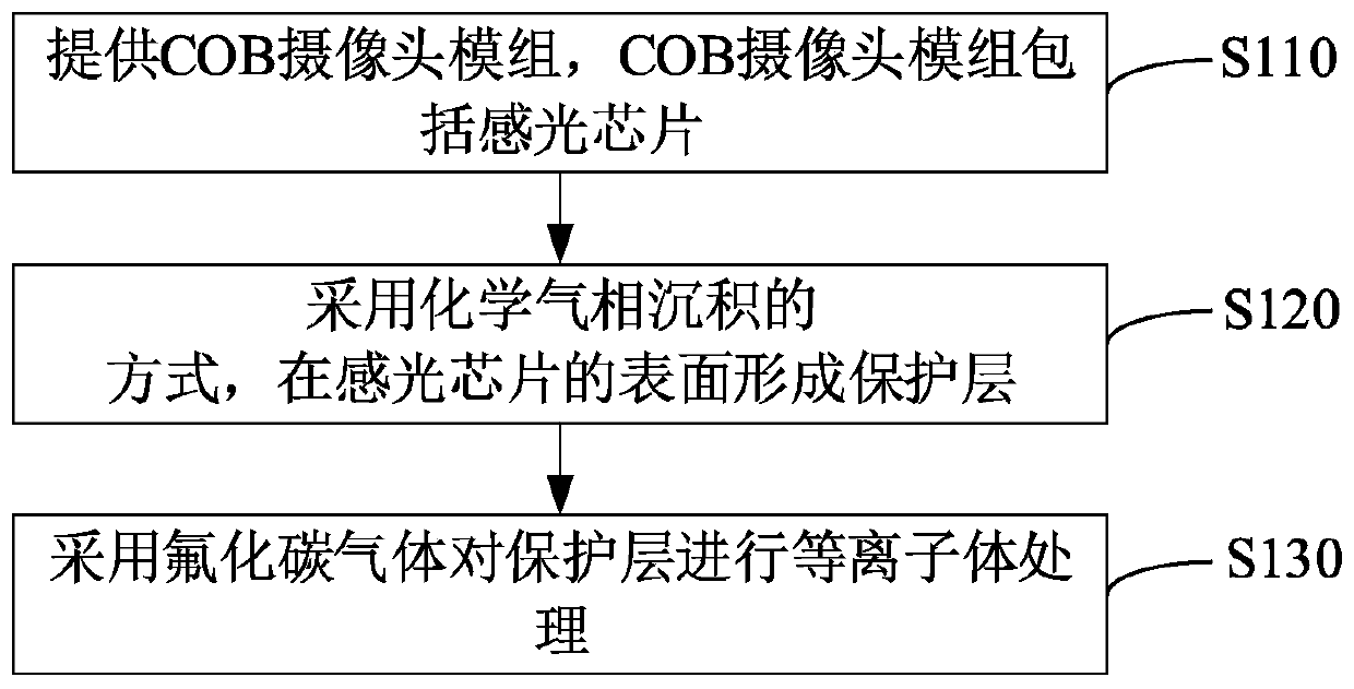
[0058] (1) Place the COB camera module in a vacuum chamber, evacuate to 0.1Pa, and heat the COB camera module to 45°C. Then introduce parylene C-type monomer, after vaporization, pyrolysis, and chemical deposition for 15 minutes, a parylene protective layer with a thickness of 0.1 μm is obtained on the surface of the photosensitive chip.

[0059] (2) Assemble the bracket and the lens in the COB camera module on the PCB board respectively, adjust the focus and fix the lens, and complete the packaging of the COB camera module.

Embodiment 2

[0061] (1) Place the COB camera module in a vacuum chamber, evacuate to 5.0Pa, and heat the COB camera module to 100°C. Then, styrene monomer was introduced, and after vaporization, pyrolysis, and chemical deposition for 300 minutes, a polystyrene protective layer with a thickness of 5.0 μm was obtained on the surface of the photosensitive chip.

[0062] (2) Plasma treatment is performed on the protective layer. Wherein, the power in the plasma treatment is 200W, and the time of the plasma treatment is 10min. The working gas in the plasma treatment is argon and C with a flow ratio of 1:1. 3 f 8 of mixed gas. After the plasma treatment, the photosensitive chip whose surface is a hydrophobic protective layer is obtained.

[0063] (3) Assemble the bracket and the lens in the COB camera module on the PCB board respectively, adjust the focus and fix the lens, and complete the packaging of the COB camera module.

Embodiment 3

[0065] (1) Place the COB camera module in a vacuum chamber, evacuate to 2.5Pa, and heat the COB camera module to 55°C. Then introduce methyl methacrylate monomer, after vaporization, pyrolysis, and chemical deposition reaction for 60 minutes, a polymethyl methacrylate protective layer with a thickness of 1.0 μm is obtained on the surface of the photosensitive chip.

[0066] (2) Plasma treatment is performed on the protective layer. Wherein, the power in the plasma treatment is 400W, and the time of the plasma treatment is 3 minutes. The working gas in the plasma treatment is argon and C with a flow ratio of 1:2. 4 f 8 of mixed gas. After the plasma treatment, the photosensitive chip whose surface is a hydrophobic protective layer is obtained.

[0067] (3) Assemble the bracket and the lens in the COB camera module on the PCB board respectively, adjust the focus and fix the lens, and complete the packaging of the COB camera module.


PUM

PropertyMeasurementUnit
Thicknessaaaaaaaaaa
Thicknessaaaaaaaaaa
Thicknessaaaaaaaaaa

Abstract

The invention relates to a COB camera module and a packaging method thereof. The packaging method of the COB camera module comprises the following steps that the COB camera module including a photosensitive chip is provided; and a protective layer is formed in the surface of the photosensitive chip by means of chemical vapor deposition. The protective layer is made of a homopolymer or copolymer, the homopolymer is one selected from parylene, polystyrene and acrylic polymers, and copolymer is formed by polymerizing at least two selected from parylene, styrene andacrylic ester monomers. According to the packaging method of the COB camera module, impurity particles are not adhered to the photosensitive chip directly in the packaging process, and the photosensitive chip is not damaged in the process of removing the impurity particles. The material of the protective layer has a high optical performance, and the protective layer has lower influence on the imaging quality of the COB camera module.

Description

technical field [0001] The invention relates to the technical field of camera modules, in particular to a COB camera module and a packaging method thereof. Background technique [0002] There are two packaging modes of traditional image modules: COB (Chip On Board) and CSP (Chip Scale Package). The advantage of CSP packaging is that the packaging section is completed by the front-end process, and because the CSP chip is covered by glass, it has lower requirements for cleanliness, better yield, low cost of process equipment, and short process time. The challenge is the light penetration rate. Poor, more expensive, higher height Z, backlight penetration ghosting. The COB process has the advantages of better image quality, lower packaging cost, and lower module height. In addition, major brand manufacturers gradually require module manufacturers to assemble and ship products using the COB process. In the future, the COB process will become the mobile phone camera module A tre...

Claims


Application Information

Patent Timeline
IPC IPC(8): H01L27/146
Inventor 苏建华
Owner SHENZHEN AOLAN TECH CO LTD
Why Eureka
Try Eureka