Magnetron components, magnetron sputtering chambers and semiconductor processing equipment

A magnetron and component technology, which is used in magnetron, sputtering, metal material coating processes, etc., can solve the problem of large corrosion degree, small corrosion degree in the central area of ​​the target, and poor uniformity of the whole target sputtering, etc. question

Active Publication Date: 2021-06-08
BEIJING NAURA MICROELECTRONICS EQUIP CO LTD
View PDF0 Cites 0 Cited by
  • Summary
  • Abstract
  • Description
  • Claims
  • Application Information

AI Technical Summary

Problems solved by technology

[0004] However, the existing magnetron assembly has the following problems: the center area of ​​the target is more corroded, and the ring edge area is less corroded, that is, the sputtering uniformity of the whole target is poor

Method used


Image

  • Magnetron components, magnetron sputtering chambers and semiconductor processing equipment
  • Magnetron components, magnetron sputtering chambers and semiconductor processing equipment

Examples


Embodiment 1

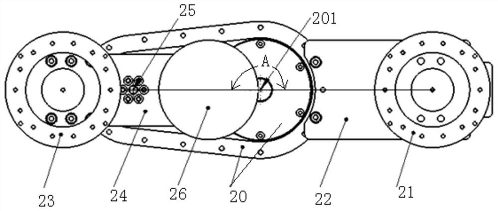
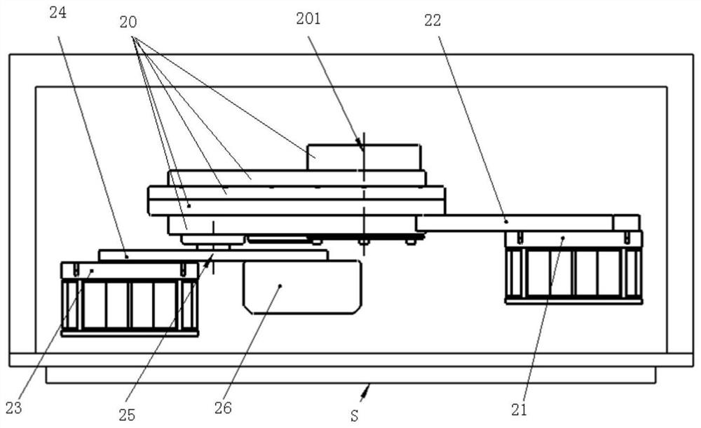
[0023] figure 1 The bottom view of the magnetron assembly provided for the embodiment of the present invention; figure 2 for figure 1 Front view of the magnetron assembly shown in application. Please also refer to Figure 1~2 , The magnetron assembly provided by the embodiment of the present invention includes: a rotating mechanism 20 , a first magnetron 21 , a first rotating arm 22 , a second magnetron 23 , a second rotating arm 24 and a rotating shaft 25 . Wherein, the rotating mechanism 20 is used to rotate along its central axis 201 under the driving of the driving mechanism; the first magnetron 21 is fixedly connected with the rotating mechanism 20 through the first rotating arm 22, so as to drive the first The magnetron 21 rotates around the central axis 201; the second magnetron 23 is fixedly connected with the second rotating arm 24, and the second rotating arm 24 is connected with the rotating mechanism 20 through the rotating shaft 25, so as to drive the second r...

Embodiment 2

[0035] An embodiment of the present invention also provides a magnetron sputtering chamber, which includes a magnetron assembly, and the magnetron assembly adopts the magnetron assembly provided in Embodiment 1 above.

[0036] The magnetron sputtering chamber provided in the embodiment of the present invention adopts the magnetron assembly provided in Embodiment 1 of the present invention, so the utilization rate of the target material and the process quality of the thin film can be improved.

Embodiment 3

[0038] An embodiment of the present invention provides a semiconductor processing device, including: the magnetron sputtering chamber provided in Embodiment 2 above.

[0039] The semiconductor processing equipment provided in the embodiment of the present invention adopts the magnetron sputtering chamber provided in the above-mentioned embodiment 2, so the utilization rate of the target material and the process quality of the thin film can be improved.


PUM


Abstract

The present invention provides a magnetron assembly, comprising: a rotating mechanism, used to rotate along its central axis driven by a driving mechanism; a first magnetron, fixedly connected to the rotating mechanism through a first rotating arm, To drive the first magnetron to rotate around the central axis when the rotating mechanism rotates; the second magnetron is fixedly connected to the second rotating arm, and the second rotating arm is connected to the rotating shaft through the rotating shaft. The mechanism is connected to drive the second magnetron to rotate around the central axis when the rotation mechanism rotates; the rotation axis can rotate on its own to drive the second magnetron to rotate around the rotation axis Axis rotation. The invention also provides a magnetron sputtering chamber and semiconductor processing equipment. The invention can improve the sputtering uniformity of the target.

Description

technical field [0001] The invention belongs to the technical field of semiconductor processing equipment, and in particular relates to a magnetron assembly, a magnetron sputtering chamber and semiconductor processing equipment. Background technique [0002] Magnetron sputtering technology introduces a magnetic field on the surface of the target cathode, and uses the magnetic field to confine charged particles to increase the plasma density to increase the sputtering rate. The working principle of magnetron sputtering is: electrons collide with argon atoms in the process gas during the process of flying to the substrate under the action of the electric field in the chamber, and the ionization generates Ar positive ions and new electrons; the new electrons fly to the substrate, Ar ions are accelerated to the cathode target under the action of an electric field, and bombard the target surface with high energy to cause sputtering of the target. Among the sputtered particles, ne...

Claims


Application Information

Patent Timeline
Patent Type & Authority Patents(China)
IPC IPC(8): H01J25/52C23C14/35
Inventor 宿晓敖侯珏赵崇军兰玥
Owner BEIJING NAURA MICROELECTRONICS EQUIP CO LTD
Why Eureka
Try Eureka