
Method for producing electronic product, and electronic product

A technology of electronic components and manufacturing methods, which is applied in the fields of fixed capacitor parts, transformer/inductor parts, inductance/transformer/magnet manufacturing, etc., and can solve the problem of residue, plating solution immersion in the ceramic element body and internal electrodes. Boundaries, corrosion, etc.

Active Publication Date: 2019-06-04
MURATA MFG CO LTD
View PDF8 Cites 0 Cited by
  • Summary
  • Abstract
  • Description
  • Claims
  • Application Information

AI Technical Summary

Problems solved by technology

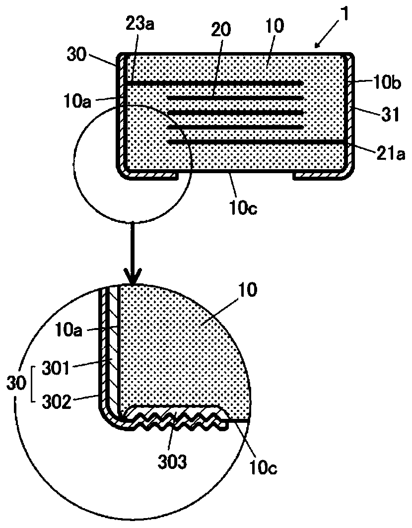
[0005] However, in this method, since the external electrode is formed by directly depositing plating on the end of the internal electrode and the anchor joint, the plating solution may infiltrate into the boundary between the ceramic element body and the end of the internal electrode or into the ceramic element. The boundary between the body and the anchor joint remains
In addition, the flux contained in the solder during assembly may infiltrate into the interface between the ceramic element body and the internal electrodes and remain
The plating solution or flux remaining in the ceramic components may become the main cause of corrosion and other problems in the use environment

Method used


Image

  • Method for producing electronic product, and electronic product
  • Method for producing electronic product, and electronic product
  • Method for producing electronic product, and electronic product

Examples


experiment example -

[0053] Hereinafter, an experimental example in which a reformed portion and a plating electrode were formed will be described.

[0054] (1) A sintered ceramic element body made of Ni-Cu-Zn-based ferrite is irradiated while scanning repeatedly with laser light. Although the processing conditions are as follows, the wavelength may be in any range from 532 nm to 10620 nm, for example. The irradiation interval refers to the distance between the forward path and the point center of the return path when scanning the laser light repeatedly.

[0055] [Table 1]

[0056] [Laser processing conditions]

[0057] wavelength

1064nm (YVO4)

Output Power

14A

scanning speed

200mm / s

Q switch frequency

20kHz

Irradiation interval (pitch)

30μm

Spot diameter

70μm

Energy Density

1J / sec

[0058] (2) The ceramic element body after laser irradiation was plated under the following conditions. Specifically, barrel platin...


PUM


Abstract

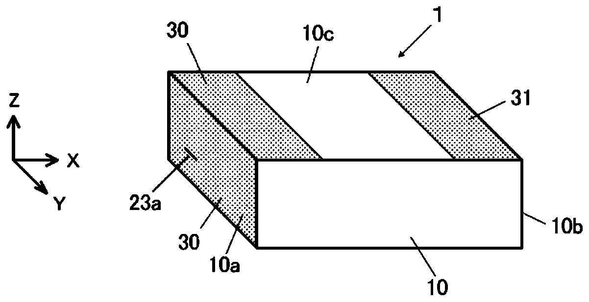
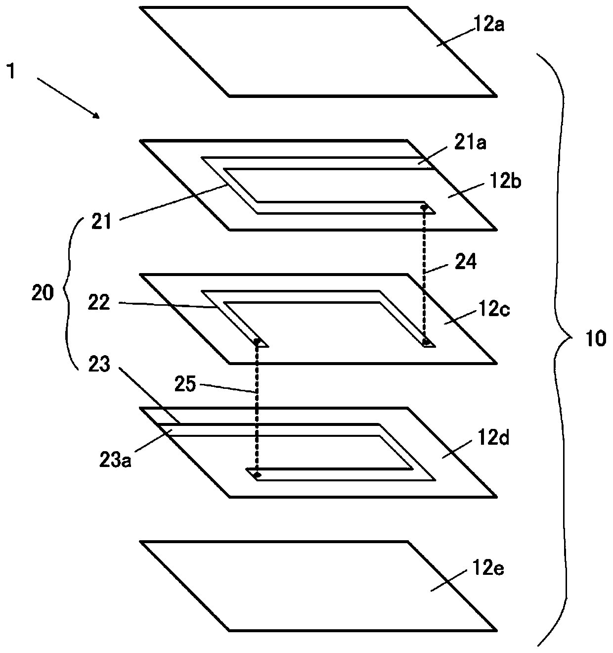
The invention is to propose a method for producing an electronic component, the method being capable of preventing the intrusion of a plating liquid or a flux component at an interface at which an internal electrode of a ceramic element body has been withdrawn, and being capable of forming an external electrode having an arbitrary shape. A ceramic element body, in which a part of an internal electrode 20 has been withdrawn at withdrawing surfaces 10a, 10b, is prepared as a ceramic element body 10 composed of a ceramic material containing a metal oxide. Then, a base electrode 301 is formed on the withdrawing surfaces of the ceramic element body through an electrode forming method using conductive paste, such that the base electrode 301 contacts the internal electrode. Next, a modified part303 is formed by locally heating a part of another surface adjacent to the withdrawing surfaces of the ceramic element body and by reducing a part of the metal oxide. Thereafter, external electrodes 30, 31 are formed by continuously forming a plating electrode 302 across the base electrode 301 and the modified part 303 through a plating method.

Description

technical field [0001] The present invention relates to a method for manufacturing an electronic component and the electronic component, and in particular to a method for forming external electrodes on a ceramic element body. Background technique [0002] In the past, the method of forming the external electrodes of electronic components is generally to apply electrode paste on both end surfaces of the ceramic element body, and then to bake or solidify the electrode paste to form a base electrode, and then to perform plating treatment on the base electrode. Thus, a plated electrode is formed. [0003] The electrode paste can be applied by a method of immersing the end of the electronic component in a paste film formed with a predetermined thickness, or a method of transferring with a roller or the like. With regard to these technologies, as a problem, it is impossible or difficult to form a special-shaped external electrode typified by an L-shaped electrode. [0004] In ad...

Claims


Application Information

Patent Timeline
Patent Type & Authority Applications(China)
IPC IPC(8): H01F41/04H01F27/29H01G4/232H01G4/30
CPCH01G4/30H01F27/292H01F17/0013H01F41/046C04B35/26H01G4/2325H01F27/2804H01F41/041C04B41/009H01G4/232C04B41/4564C04B41/88H01F41/10Y10T29/4902C04B41/5127
Inventor 间木祥文石田卓也平井真哉
Owner MURATA MFG CO LTD
Learn More