Light-emitting diode and method of making the same

A technology of light-emitting diodes and light-emitting layers, applied in semiconductor devices, electrical components, circuits, etc., can solve problems such as low carrier mobility and current congestion, reduce light absorption efficiency, increase adhesion, and reduce the risk of falling off Effect

Active Publication Date: 2021-10-19
QUANZHOU SANAN SEMICON TECH CO LTD
View PDF3 Cites 0 Cited by
  • Summary
  • Abstract
  • Description
  • Claims
  • Application Information

AI Technical Summary

Problems solved by technology

In GaN LEDs, p-GaN usually causes some current congestion at the bottom of the pad due to its low carrier mobility

Method used


Image

  • Light-emitting diode and method of making the same
  • Light-emitting diode and method of making the same
  • Light-emitting diode and method of making the same

Examples


Embodiment 1

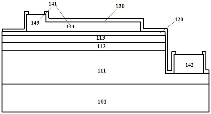
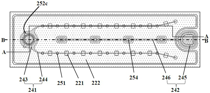
[0082] see Figure 3-5 ,in image 3 shows a top view of a light emitting diode according to a first preferred embodiment of the present invention, Figure 4 is along image 3 A side sectional view taken along the line A-A, Figure 5 is along image 3 A side sectional view taken along the line B-B. The LED comprises: a substrate 201 , an N-type layer 211 , a light-emitting layer 212 , a P-type layer 213 , an insulating layer 221 , a transparent conductive layer 230 , a protective layer 222 , a first electrode 241 , and a second electrode 242 . The first electrode 241 includes a pad 243 and an extension 244 , and the second electrode 242 includes a pad 245 and an extension 246 .

[0083] Specifically, the substrate 201 includes but is not limited to sapphire, aluminum nitride, gallium nitride, silicon, and silicon carbide, and its surface structure can be a planar structure or a patterned pattern structure; the N-type layer 211 is formed on the sapphire substrate 201 the l...

Embodiment 2

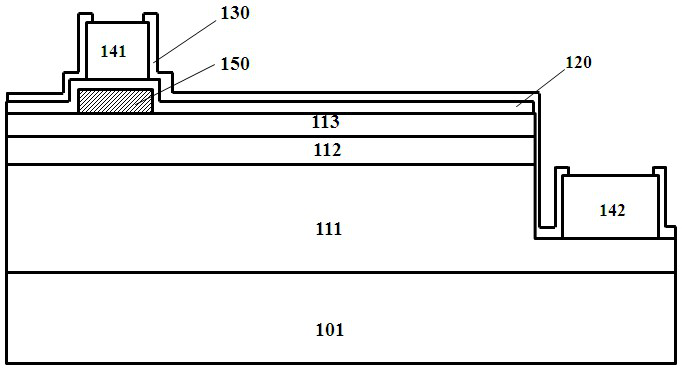
[0098] Figure 9 with 10 A schematic diagram showing the structure of another light-emitting diode, where Figure 9 for top view, Figure 10 for along Figure 9 Sectional view cut by line A-A. The difference from Embodiment 1 is that in the light emitting diode structure described in this embodiment, the insulating layer 221 under the first electrode 241 is connected together, so that the current injection under the electrode can be completely avoided, and the height of the first electrode extension part 244 can be reduced. All of them are raised, and the refraction effect can be used to effectively reduce the metal light blocking area of ​​the electrode extension, thereby improving the light extraction efficiency of the LED.

Embodiment 3

[0100] Figure 11-12 A schematic diagram of the structure of another light-emitting diode is shown, where Figure 11 for top view, Figure 12 for along Figure 11 Sectional view cut by line A-A. The difference from Embodiment 1 is that in the light-emitting diode structure described in this embodiment, under the extension portion 244 of the first electrode, the insulating layer 221 overlaps with the opening 251 of the protective layer 222, and the area of ​​the insulating layer 221 is smaller than that of the opening. 251 square meters. Figure 13 Shown is a partially enlarged view of the extension 244 of the first electrode. The transparent conductive layer 230 forms a gap between the opening 251 and the protective layer 222. The extension 244 of the first electrode fills the gap. On the one hand, the first electrode is in the insulating layer. The position of 221 forms a nail pile structure, which increases the adhesion between the electrode extension 244 and the protect...


PUM

PropertyMeasurementUnit
thicknessaaaaaaaaaa

Abstract

The invention discloses a light-emitting diode and a manufacturing method thereof. In some embodiments, the light-emitting diode includes: a light-emitting epitaxial layer, which sequentially includes a first semiconductor layer, a light-emitting layer, and a second semiconductor layer from top to bottom. The upper surface is provided with a first electrode region, which includes a pad region and an extension region; an insulating layer is formed on the extension region of the first semiconductor layer; a transparent conductive layer is formed on the surface of the first semiconductor layer and cover the insulating layer; a protective layer is formed on the surface of the transparent conductive layer, and a first opening is formed in the extended region, exposing part of the surface of the transparent conductive layer in the extended region; a first electrode, Formed on the protection layer, including a pad portion and an extension portion, the extension portion forms an electrical connection with the transparent conductive layer of the extension area through the first opening.

Description

technical field [0001] The invention relates to a semiconductor element, in particular to a light emitting diode and a manufacturing method thereof. Background technique [0002] Due to the advantages of long life, small size, high shock resistance, low heat generation and low power consumption, light-emitting diodes have been widely used in home appliances and indicators or light sources of various instruments. [0003] The early gallium nitride LED chip manufacturing process usually consists of four processes: mesa etching (MESA), making a transparent conductive layer (such as ITO), making electrodes and making a protective layer. The light-emitting diode chips formed by it are as follows: figure 1 As shown, it generally includes a substrate 101, an N-type layer 111, a light emitting layer 112, a P-type layer 113, a transparent conductive layer 120, a P electrode 141 (pad 143 and an extension bar 144), an N electrode 142 and a protective layer 130. In GaN LEDs, p-GaN typi...

Claims


Application Information

Patent Timeline
Patent Type & Authority Patents(China)
IPC IPC(8): H01L33/00H01L33/14H01L33/36H01L33/44H01L33/46
CPCH01L33/145H01L33/387H01L33/62H01L33/46H01L33/14H01L33/36H01L33/38H01L33/44H01L33/382H01L2933/0016H01L2933/0025H01L33/405
Inventor 林素慧王锋洪灵愿许圣贤陈思河陈大钟彭康伟张家宏
Owner QUANZHOU SANAN SEMICON TECH CO LTD
Why Eureka
Try Eureka