Magnetic field assisted chemical etching device and method

A chemical etching and magnetic field-assisted technology, which is applied in the direction of electrical components, semiconductor/solid-state device manufacturing, circuits, etc., can solve problems such as high cost, limited application range, and complicated operation, and achieve low cost, improved etching rate, Apply a wide range of effects

Inactive Publication Date: 2019-06-07
SUZHOU JUZHEN PHOTOELECTRIC
View PDF7 Cites 2 Cited by
  • Summary
  • Abstract
  • Description
  • Claims
  • Application Information

AI Technical Summary

Problems solved by technology

[0004] Therefore, the technical problem to be solved by the present invention is to overcome the defects of limited application range, complicated operation and high cost of the prior art using magnetic field controlled chemical etching method, so as to provide a kind of etching method with wide application range, simple operation and low cost, and etching A Magnetic Field Assisted Chemical Etching Method with High Pattern Accuracy and Efficiency
[0005] Another technical problem to be solved by the present invention is to overcome the defects of limited application range, complicated operation and high cost of the prior art using a magnetic field control chemical etching device, so as to provide a wide application range, simple operation and low cost, and an etching A magnetic field assisted chemical etching device with high pattern accuracy and efficiency

Method used


Image

  • Magnetic field assisted chemical etching device and method
  • Magnetic field assisted chemical etching device and method
  • Magnetic field assisted chemical etching device and method

Examples


Embodiment 1

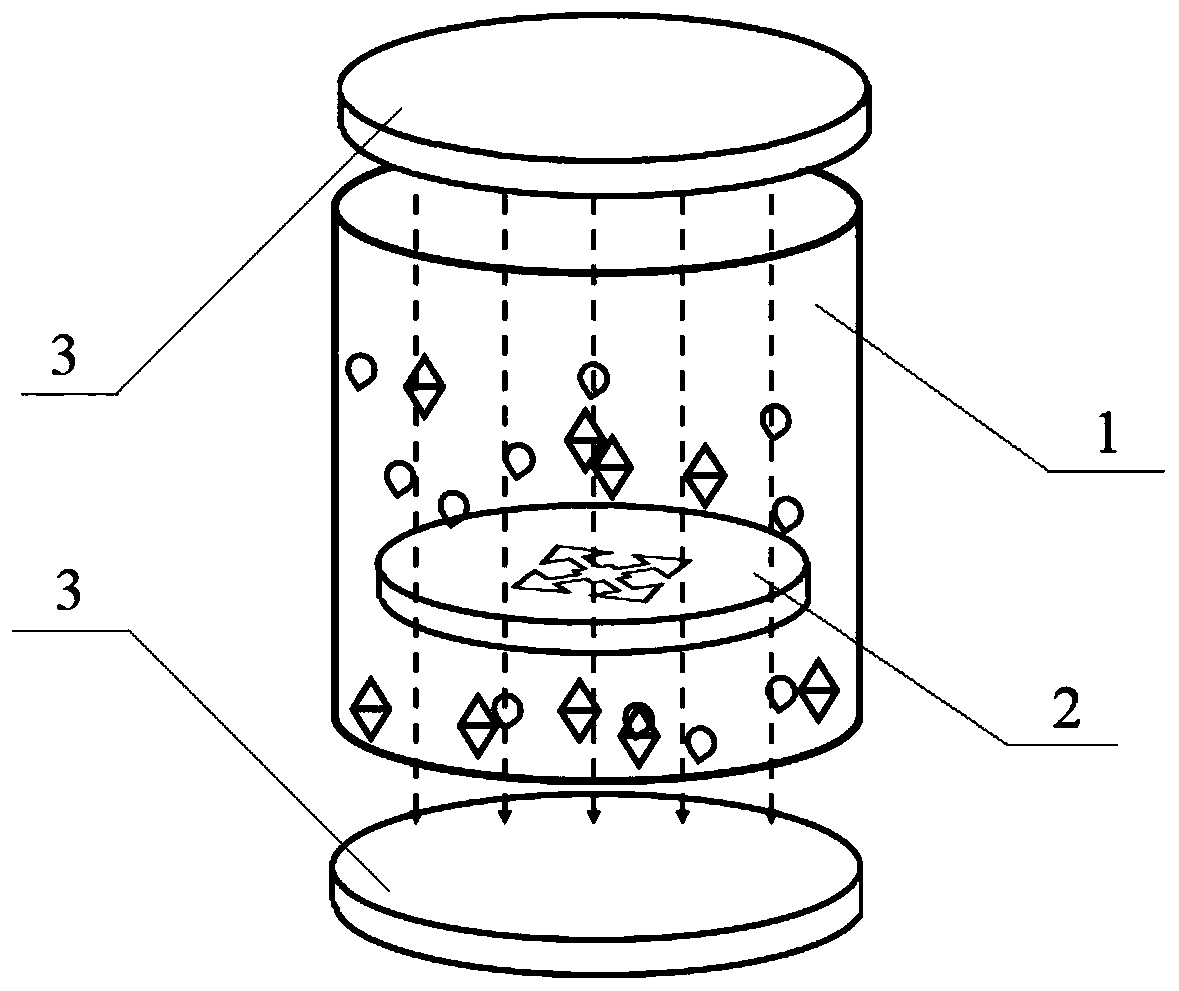
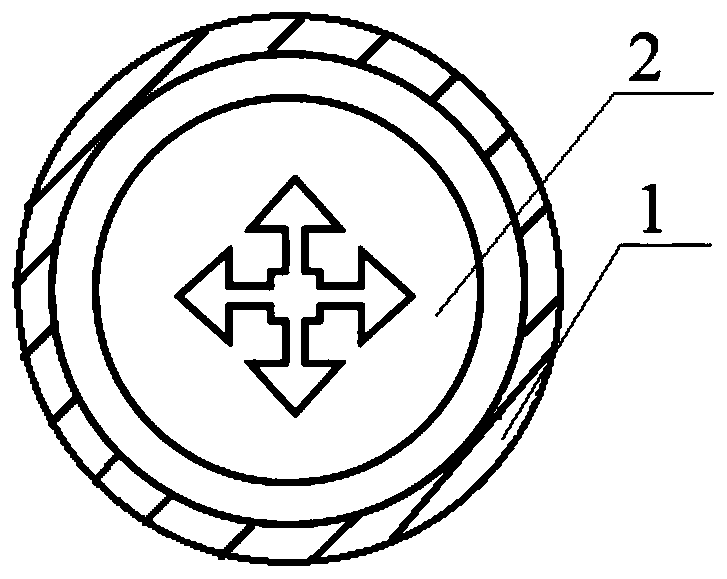
[0038] This embodiment provides a device for magnetic field-assisted chemical etching, including a solution bottle 1 to accommodate the etching solution and the material to be etched 2, which is arranged outside the solution bottle 1 to provide a stable magnetic field for magnetic field excitation device, the magnetic field excitation device is two magnets 3 with opposite polarities arranged oppositely, and the magnets 3 are composed of permanent magnets.

[0039] A method for magnetic field-assisted chemical etching utilizing the above-mentioned device, comprising:

[0040] S1. Take a semiconductor material with a size of Φ100mm×200μm. The semiconductor material is a GaAs semiconductor substrate. Use a DY-220SP polishing machine and a DY-220SG grinding machine to polish the substrate, and then use deionized water and acetone to ultrasonically clean it for 5 minutes. , with N 2 blow dry. After the substrate was cleaned and dried, it was placed on an ATJ-100 coater, and AZ926...

Embodiment 2

[0044] The magnetic field-assisted chemical etching is performed using a device similar to that of Example 1, except that the magnet is composed of an electromagnetic coil.

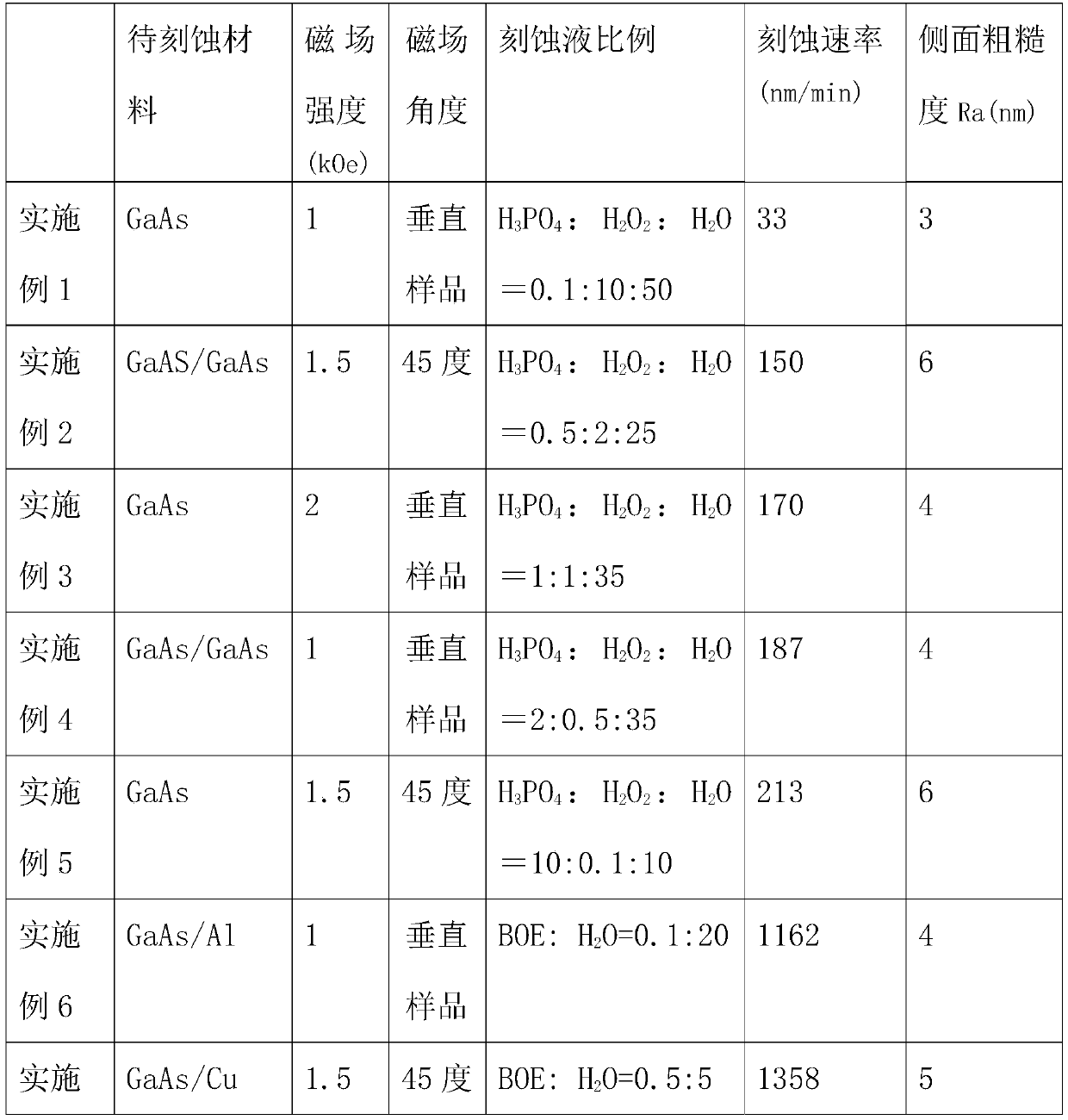
[0045] The magnetic field assisted chemical etching is carried out in a method similar to that of Example 1, the difference is that in the S1 step, the semiconductor material used is composed of a GaAs semiconductor substrate and a GaAs epitaxial layer, wherein the GaAs epitaxial layer covers the GaAs semiconductor substrate the upper surface of the sheet; in the S2 step, inject H into the solution bottle 3 PO 4 、H 2 o 2 、H 2 O: 300ml of etching solution with a volume ratio of 0.5:2:25; the adjusted magnetic field strength is 1.5kOe, and the direction of the magnetic field faces the bottom of the solution bottle and is at 45 degrees to the bottom of the solution bottle.

[0046] The material obtained after etching was taken out, rinsed with deionized water for 2 min, and then washed with N 2 Blow dry...

Embodiment 3

[0048] The same apparatus as in Example 1 was used for magnetic field assisted chemical etching.

[0049] Carry out magnetic field-assisted chemical etching in a method similar to Example 1, the difference is that, in the S2 step, inject H into the solution bottle 3 PO 4 、H 2 o 2 、H 2 O is 300ml of etching solution with a volume ratio of 1:1:35; the adjusted magnetic field strength is 2kOe.

[0050] The material obtained after etching was taken out, rinsed with deionized water for 2 min, and then washed with N 2 Blow dry, use the ZYGO optical interferometer test system, measure the etching depth and the side roughness of the remaining pattern after etching, and calculate the etching rate. The obtained etch rate and the roughness results of the side of the retained pattern are shown in Table 1.


PUM


Abstract

The invention provides a magnetic field assisted chemical etching method. The method includes the following steps: S1, performing gluing and photo etching processing on a semiconductor material so that a to-be-etched material can be obtained; and S2, putting the to-be-etched material into an etching liquid, and performing etching under a magnetic field with the intensity being 1 kOe - 2 kOe. A magnetic field assisted chemical etching device is also provided. The device includes a solution bottle and a magnetic field excitation device; the solution bottle is used for accommodating the etching liquid and the to-be-etched material; and the magnetic field excitation device is arranged at the external of the solution bottle and used for providing a stable magnetic field. Through the addition ofconventional chemical etching and the magnetic field, anions and cations in the etching solution can move along a certain direction, so that directional etching can be realized, damages to the side surfaces of retained graphics can be reduced, the moving ions can be accelerated, and etching rates can be enhanced; and the method is simple in operation, low in cost and wide in application range, and can realize the directional chemical etching of all common semiconductor chips at the present stage.

Description

technical field [0001] The invention relates to the field of semiconductors, in particular to a device and method for magnetic field assisted chemical etching. Background technique [0002] In recent years, semiconductor lasers have developed rapidly and have been successfully applied in information communication, aerospace, medical treatment, material science and other fields. The new technology field has high requirements for semiconductor laser materials, processes, and packaging levels. Among them, the dimensional accuracy of the internal graphics of the chip and the thin film is the key factor affecting the performance of the device. Therefore, how to accurately, efficiently and cost-effectively prepare accurate Reliable graphics become the key to research. In the prior art, the etching method is often used to process the semiconductor material after photolithography and development. The unexposed part is not etched because it is covered by photoresist after developmen...

Claims


Application Information

Patent Timeline
Patent Type & Authority Applications(China)
IPC IPC(8): H01L21/306H01L21/67
Inventor 丁雪峰沈雷
Owner SUZHOU JUZHEN PHOTOELECTRIC
Why Eureka
Try Eureka