Method for making array micro-table-board of idium-gallium-arsenium coke plane detector

A focal plane detector, indium gallium arsenic technology, applied in semiconductor devices, final product manufacturing, sustainable manufacturing/processing, etc., can solve material lattice damage, poor passivation effect and anti-reflection effect, device performance degradation, etc. problem, to achieve the effect of reducing side damage, improving long-term stability and reliability, and improving graphic fidelity

Inactive Publication Date: 2008-06-04
SHANGHAI INST OF TECHNICAL PHYSICS - CHINESE ACAD OF SCI
View PDF2 Cites 0 Cited by
  • Summary
  • Abstract
  • Description
  • Claims
  • Application Information

AI Technical Summary

Problems solved by technology

The advantages of dry etching are: high pattern transfer accuracy, good anisotropy and controllability; but the disadvantage is: dry etching will cause damage to the material lattice and reduce device performance
Although SiO 2 、SiN x The inorganic dielectric film is in good contact with InP and InGaAs, which can effectively reduce the recombination of the minority carrier surface. However, due to factors such as growth conditions, the growth layer on the mesa surface is often thicker, and the side growth layer is thinner. Smooth, so the effect of the passivation film grown on the side is poor, it cannot effectively reduce the dark current, and cannot guarantee the long-term working stability of the device
Organic dielectric film polyimide has the advantages of corrosion resistance, radiation resistance, high temperature resistance, and good adhesion, but the passivation effect and anti-reflection effect are poor. Devices passivated by this method have higher requirements for detection rate and response rate. High space remote sensing detectors are still far behind

Method used


Image

  • Method for making array micro-table-board of idium-gallium-arsenium coke plane detector
  • Method for making array micro-table-board of idium-gallium-arsenium coke plane detector

Examples


Embodiment Construction

[0016] Below in conjunction with accompanying drawing and embodiment the concrete implementation method of the present invention is described in further detail:

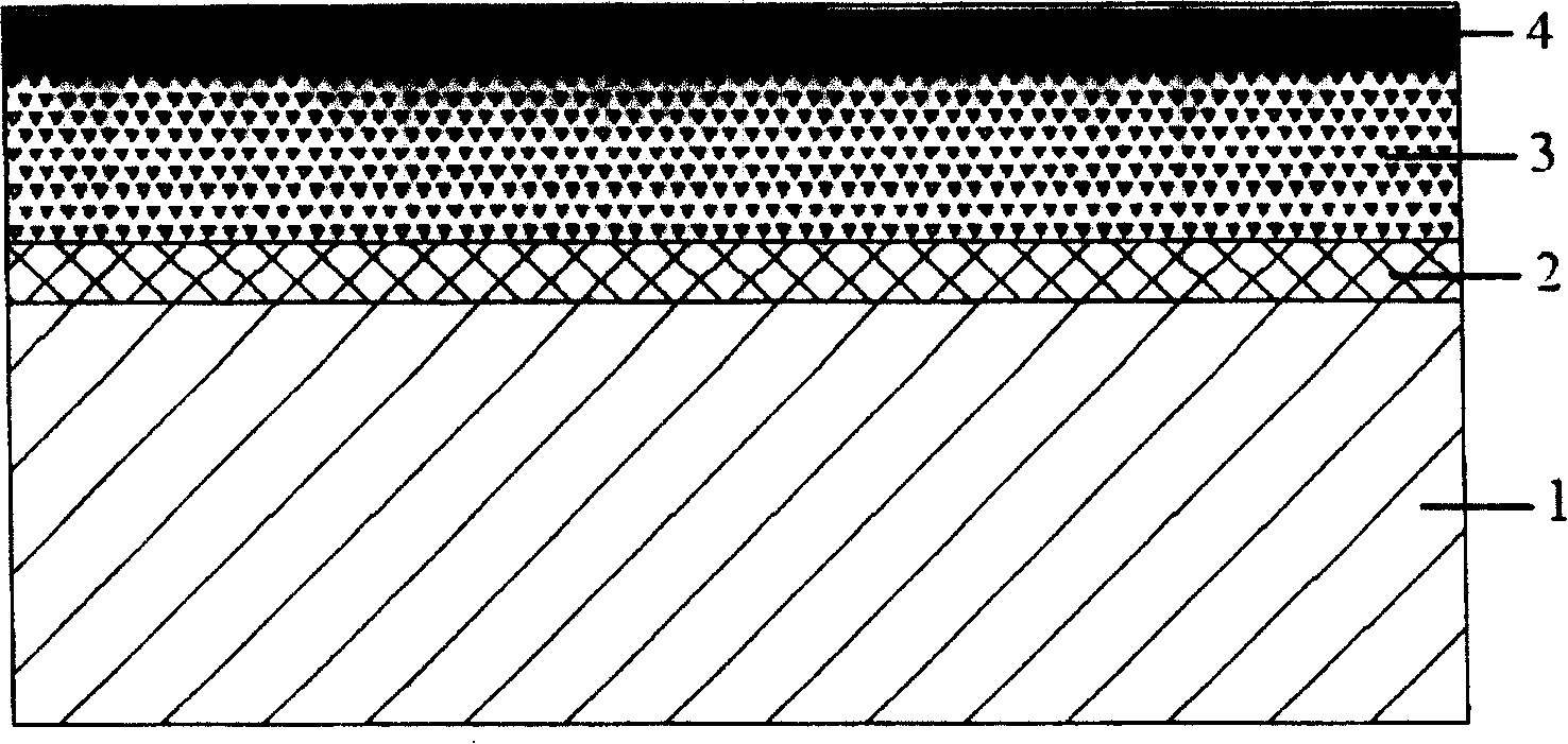
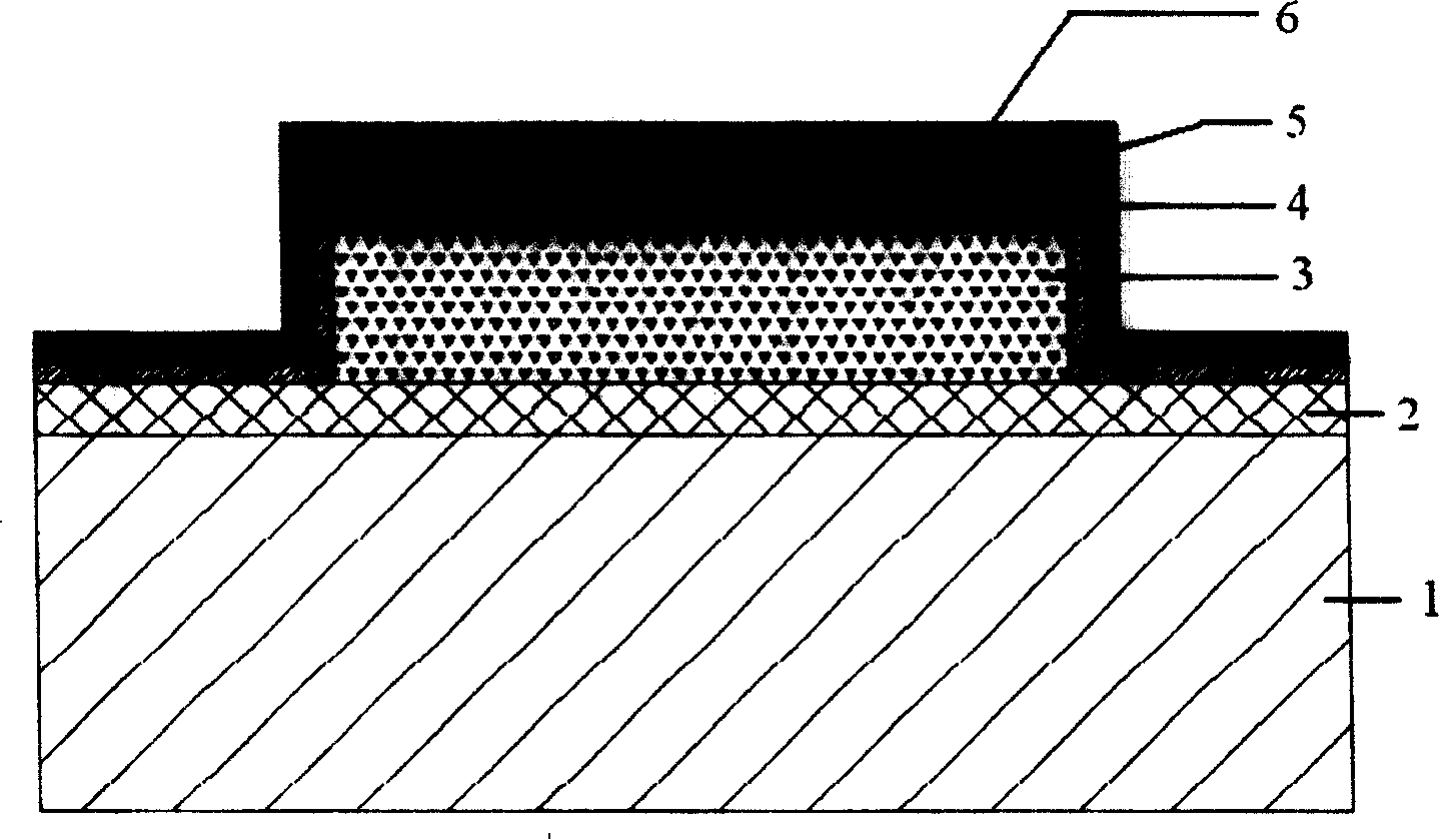
[0017] Preparation of epitaxial materials: N-type InP layer 2 with a thickness of 1 μm is sequentially grown on a semi-insulating InP substrate 1 with a thickness of 350 μm by molecular beam epitaxy technology, and the carrier concentration is greater than 2×10 18 cm -3 ; In with a thickness of 2.5 μm 0.53 Ga 0.47 As absorption layer 3; P-type InP layer 4 with a thickness of 0.5 μm and a carrier concentration greater than 2×10 18 cm -3 .

[0018] The specific preparation steps of micro-mesas and passivation layer are as follows:

[0019] 1. The above-mentioned epitaxial materials were ultrasonically cleaned with chloroform, diethyl ether, acetone, and ethanol in sequence, for more than 2 minutes each time, and dried with nitrogen gas.

[0020] 2. Positive photolithography, drying at 65°C for 40 minutes after ph...


PUM


Abstract

This invention discloses a preparation method for an array micro-mesa of an InGaAs focal plane, which first of all uses an Ar+ ionic drying method to etch a P-type InP layer, then uses a wet method to corrode the InGaAs absorption layer to either increase the fidelity factor of the graph of the photosensitive face or reduce the side harm of the InGaAs absorption, removes the surface oxidation layer by a sulfuration process and covers a new ZnS / polyimide double passivation film.

Description

technical field [0001] The present invention relates to the preparation technology of indium gallium arsenide (InGaAs) focal plane detector, specifically refers to the preparation method of array micro-mesas of InP / InGaAs / InP focal plane detector, and this method comprises: the formation of array micro-mesas and in A method for forming a second passivation layer on a micro-mesa. Background technique [0002] At present, most of the array micro-mesas of InP / InGaAs / InP focal plane detectors adopt selective wet chemical etching, and a few adopt dry etching. Wet chemical etching: when etching the InP layer, HCl / H is generally used 2 O series and HCl / H 3 PO 4 It is an etching solution. When etching the InGaAs layer, H 2 SO 4 / H 2 o 2 / H 2 O series, H 3 PO 4 / H 2 o 2 / H 2 O series and tartaric acid / H 2 o 2 / H 2 O series corrosive liquid. The test shows that when the InP layer is corroded, due to the use of strong acid, it has a corrosive effect on the photoresist,...

Claims


Application Information

Patent Timeline
Patent Type & Authority Patents(China)
IPC IPC(8): H01L31/18
CPCY02P70/50
Inventor 吕衍秋韩冰李萍庄春泉吴小利陈江峰龚海梅
Owner SHANGHAI INST OF TECHNICAL PHYSICS - CHINESE ACAD OF SCI
Why Eureka
Try Eureka