
A kind of thin film growth system and growth method

A thin-film growth and thin-film technology, applied in metal material coating process, coating, gaseous chemical plating, etc., can solve the problems of unusable thin film, sample contamination, insufficient growth of crystalline thin film, etc., to expand the scope of application, grow sufficient effect

Active Publication Date: 2021-10-15
JIAXING KEMIN ELECTRONICS EQUIP TECH
View PDF11 Cites 0 Cited by
  • Summary
  • Abstract
  • Description
  • Claims
  • Application Information

AI Technical Summary

Problems solved by technology

[0005] In view of the above-mentioned technical problems, the purpose of the present invention is to provide a thin film growth system and growth method, which integrates the functions of atomic layer deposition and annealing, and solves the problem of completing atomic layer deposition and annealing in different equipment. The technical problems of insufficient growth of crystalline thin films and sample contamination are solved. At the same time, the existing atomic layer deposition equipment cannot be used for the growth of thin films with a large difference between the source temperature of the sample adsorption precursor and its reaction temperature.

Method used


Image

  • A kind of thin film growth system and growth method
  • A kind of thin film growth system and growth method

Examples


Embodiment 1

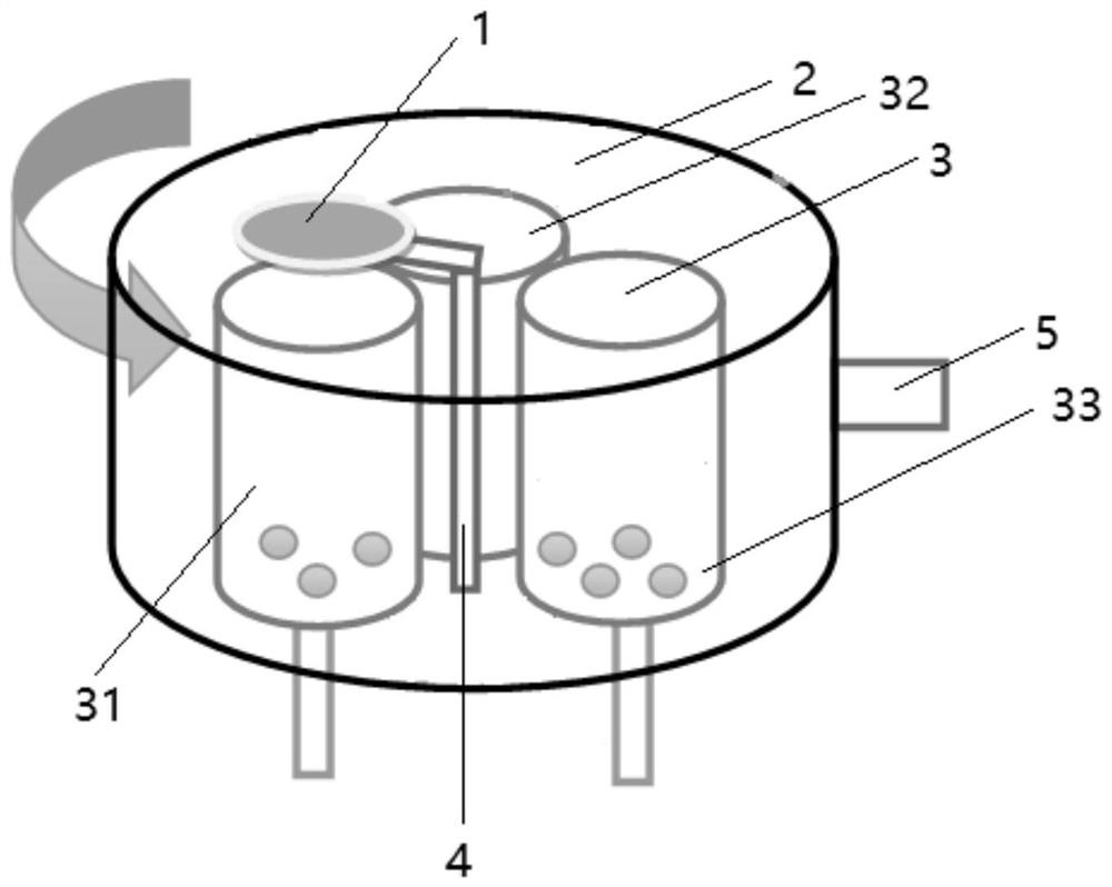
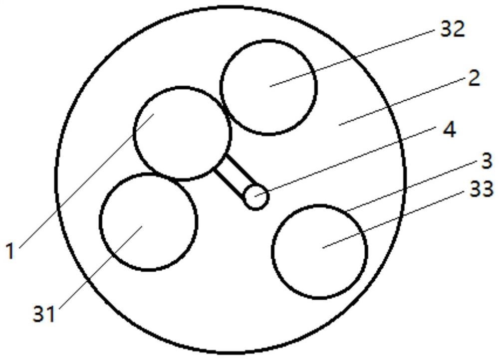
[0047] A thin film growth system, comprising a sample chamber, a large chamber, a plurality of small chambers, and a central axis, the plurality of small chambers are located in the large chamber, and the central axis is located in the center of the axis of the large chamber, The sample chamber is connected to the central shaft through a cross bar, and is used to transfer the sample in the sample chamber, and the transfer of the sample includes transferring between the plurality of small chambers, and / or, in the Transfer between the small chamber and the large chamber; the plurality of small chambers include a first small chamber and a second small chamber and an annealing chamber, and the first small chamber and the second small chamber The bottom of the chamber is provided with an openable and closable through hole, which is used to feed the precursor.

[0048] Specifically, in order to transfer the sample in the sample chamber between a plurality of small chambers, the radi...

Embodiment 2

[0050] S1. Start the vacuum pump, put the large chamber and the annealing chamber in a vacuum state, heat the small chamber so that the temperature of the first small chamber is 100°C, the temperature of the second small chamber is 300°C, and the annealing chamber The temperature is 800°C;

[0051] S2. Place the sample chamber in the first small chamber, put the silicon wafer into the sample chamber, and fill the first small chamber with the precursor trimethylaluminum, so that the silicon wafer is placed in the precursor trimethylaluminum Carry out saturated adsorption in the base aluminum to obtain the first sample;

[0052] S3. Transfer the sample chamber containing the first sample from the first small chamber to the large chamber through the central shaft, and blow nitrogen gas into the large chamber for purging, the During the purging process, the vacuum pump discharges the nitrogen gas to obtain a second sample;

[0053] S4. Transfer the sample chamber containing the ...

Embodiment 3

[0058] S1. Start the vacuum pump to make the large chamber and the annealing chamber in a vacuum state, heat the small chamber so that the temperature of the first small chamber is 80°C, the temperature of the second small chamber is 130°C, and the annealing chamber The temperature is 500°C;

[0059] S2. Place the sample chamber in the first small chamber, put quartz glass into the sample chamber, and fill the first small chamber with the precursor copper hexafluoroacetylacetonate, so that the quartz glass is placed in the precursor six Copper fluoroacetylacetonate is subjected to saturated adsorption to obtain the first sample;

[0060] S3. Transfer the sample chamber containing the first sample from the first small chamber to the large chamber through the central axis, and blow argon gas into the large chamber for purging. During the purging process, the vacuum pump discharges the argon to obtain a second sample;

[0061] S4. Transfer the sample chamber containing the seco...


PUM


Abstract

The invention relates to a film growth system and a growth method, belonging to the field of material preparation; comprising a sample chamber, a large chamber, a plurality of small chambers, and a central axis, the plurality of small chambers are located in the large chamber, and the The central axis is located at the center of the large chamber axis, and the sample chamber is connected to the central axis through a cross bar for transferring the sample in the sample chamber. Transfer between, and / or, transfer between the small chamber and the large chamber; the plurality of small chambers include a first small chamber and a second small chamber and an annealing chamber, and the first small chamber A small chamber and the bottom of the second small chamber are provided with openable and closable through holes; the system provided by the present invention has the functions of atomic layer deposition and annealing at the same time, and can prepare samples with a large difference between the source temperature and reaction temperature of the sample adsorption precursor. Thin films, expanding the application range of atomic layer deposition equipment.

Description

technical field [0001] The invention belongs to the field of material preparation, and in particular relates to a film growth system and a growth method. Background technique [0002] At present, the main methods of growing thin films are physical methods and chemical methods. Physical methods mainly include vacuum evaporation, magnetron sputtering and ion plating, etc., and chemical methods mainly include chemical vapor deposition and atomic layer deposition. Atomic layer deposition is a method of introducing the precursor source colloid into the cavity for chemical reaction to deposit thin films on the surface of the substrate. At present, it is mainly used in semiconductors, optoelectronic materials, integrated circuits and copper interconnection seed layers. Atomic layer deposition has the advantages of good shape retention and controllability of film thickness, but at present, the films of atomic layer deposition are mainly amorphous. To convert the film into a crystall...

Claims


Application Information

Patent Timeline
Patent Type & Authority Patents(China)
IPC IPC(8): C23C16/455C23C16/56
Inventor 夏洋
Owner JIAXING KEMIN ELECTRONICS EQUIP TECH
Learn More