

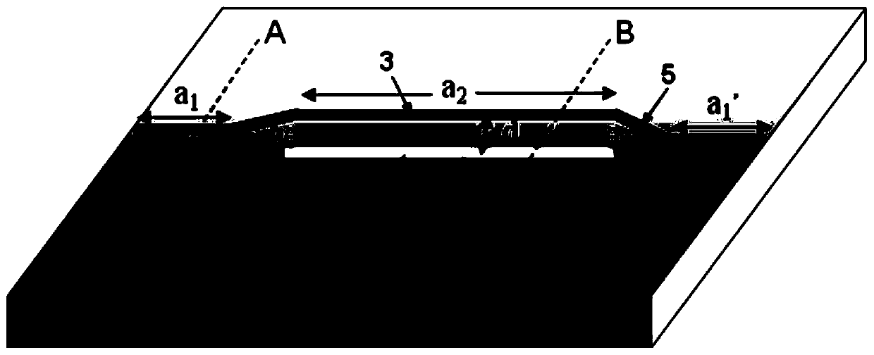
Asymmetric MZI optical waveguide-based temperature sensor and preparation method thereof
A temperature sensor and optical waveguide technology, applied in the direction of physical/chemical change thermometers, light guides, thermometers, etc., can solve the problems of losing temperature sensing function and limiting the practical application of temperature sensors with MZI optical waveguide structure, and achieve the goal of being suitable for large Large-scale production, low production cost, and large thermo-optic coefficient
- Summary
- Abstract
- Description
- Claims
- Application Information
AI Technical Summary
Problems solved by technology
Method used
Image

Examples
Embodiment 1
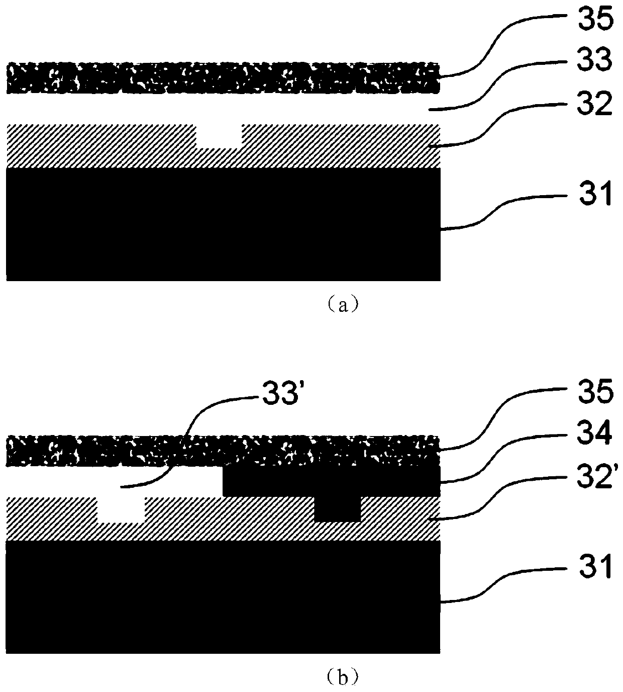
[0045] Cleaning treatment of silicon substrate: Soak the silicon substrate in acetone solution and ultrasonically clean it for 8 minutes, then repeatedly wipe it with acetone and ethanol cotton balls in sequence, rinse it with deionized water, dry it with nitrogen, and finally put it under the condition of 110°C Bake for 1.5 hours to remove moisture.
[0046] The lower cladding of the polymer waveguide was prepared by spin-coating: the polymer material PMMA was spin-coated on the cleaned silicon substrate, the spin-coating speed was controlled at 3000 rpm, and then the film was baked at 120°C for 2.5 hours , to obtain a waveguide lower cladding with a thickness of 4 μm.
[0047]The waveguide groove was prepared by standard photolithography and dry etching process: first, a layer of Al mask with a thickness of 100nm was evaporated on the prepared polymer lower cladding layer, and the Al film was spin-coated by spin-coating process. A layer of positive photoresist BP212 with a ...
Embodiment 2
[0053] Cleaning treatment of silicon substrate: Soak the silicon substrate in acetone solution and ultrasonically clean it for 8 minutes, then repeatedly wipe it with acetone and ethanol cotton balls in sequence, rinse it with deionized water, dry it with nitrogen, and finally put it under the condition of 110°C Bake for 1.5 hours to remove moisture.
[0054] The lower cladding of the polymer waveguide was prepared by spin-coating: the polymer material PMMA was spin-coated on the cleaned silicon substrate, the spin-coating speed was controlled at 3000 rpm, and then the film was baked at 120°C for 2.5 hours , to obtain a waveguide lower cladding with a thickness of 4 μm.
[0055] The waveguide groove was prepared by standard photolithography and dry etching process: first, a layer of Al mask with a thickness of 100nm was evaporated on the prepared polymer lower cladding layer, and the Al film was spin-coated by spin-coating process. A layer of positive photoresist BP212 with a...
PUM
| Property | Measurement | Unit |
|---|---|---|
| Thickness | aaaaa | aaaaa |
| Thickness | aaaaa | aaaaa |
| Thickness | aaaaa | aaaaa |
Abstract
Description
Claims
Application Information