Memory cell structure of SRAM

A storage unit and node technology, applied in information storage, static memory, digital memory information and other directions, can solve the problem of lack of anti-soft error, improve read static noise tolerance, improve anti-soft error ability, reduce leakage power consumption effect

Active Publication Date: 2019-06-14
SHANGHAI HUAHONG GRACE SEMICON MFG CORP
View PDF3 Cites 2 Cited by
  • Summary
  • Abstract
  • Description
  • Claims
  • Application Information

AI Technical Summary

Problems solved by technology

Depend on figure 1 It can be seen that when any one of the Q node and QN node is disturbed, it is easy to flip, and this structure does not have the ability to resist soft errors

Method used


Image

  • Memory cell structure of SRAM
  • Memory cell structure of SRAM
  • Memory cell structure of SRAM

Examples


Embodiment Construction

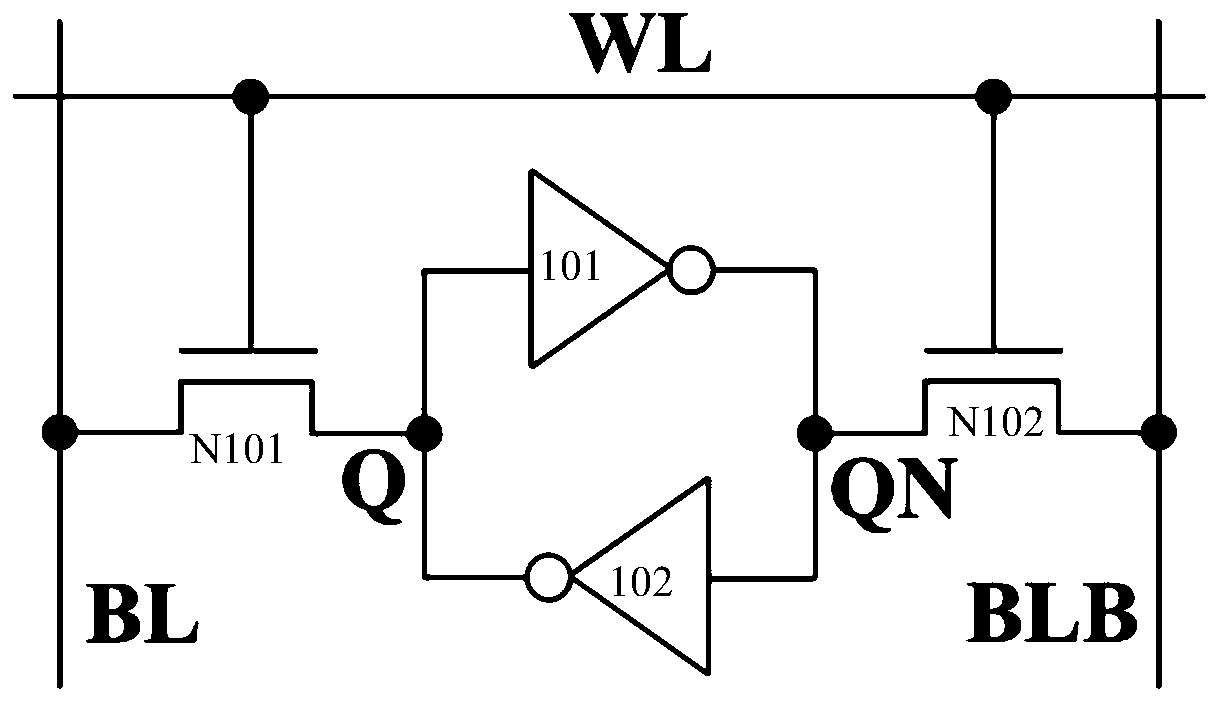
[0033] The existing second SRAM memory cell structure:

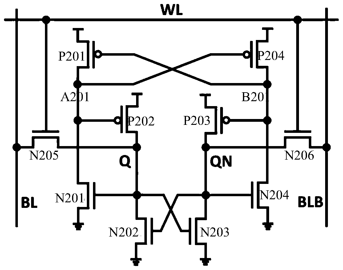
[0034] Such as figure 2 As shown, it is the memory cell structure of the second existing SRAM, including: a main structure formed by connecting NMOS transistors N201, N202, N203 and N204 and PMOS transistors P201, P202, P203 and P204, and NMOS transistors N205 and N206 are two The Q node is connected to the bit line BL through the NMOS transistor N205, the QN node is connected to the bit line BLB through the NMOS transistor N206, and the gates of the NMOS transistors N205 and N206 are both connected to the bit line WL. Q node and QN node are out of phase, Q node and B node are in phase, and A201 node and B201 node are out of phase. figure 2 The main structure shown can realize double interlocking of storage nodes and has the ability to resist soft errors. However, it still has the defect of large leakage power consumption.

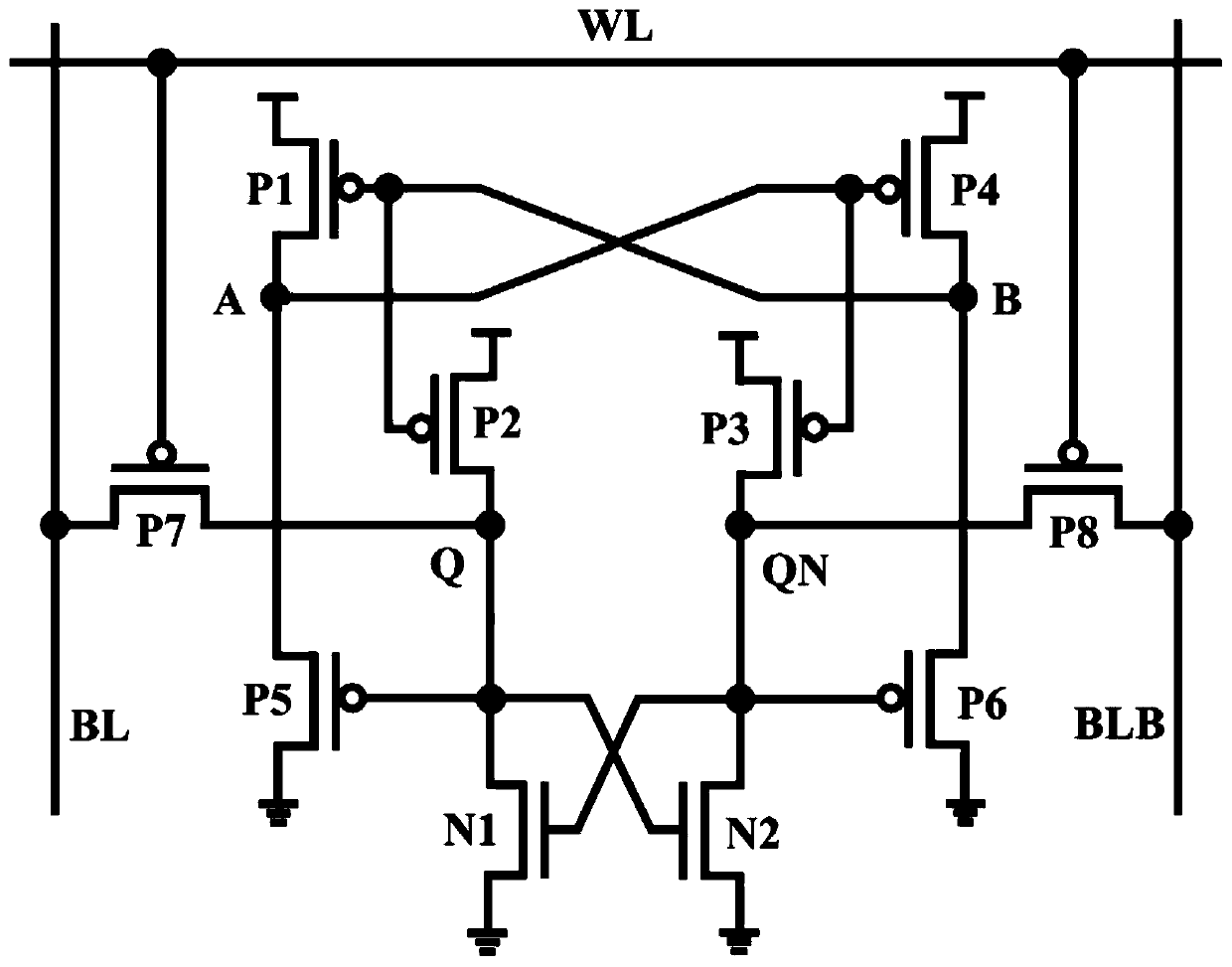
[0035] The memory cell structure of the embodiment of the present invention SRAM:

[0036] ...


PUM


Abstract

The invention discloses a memory cell structure of an SRAM (static random access memory), a main body structure consists of two NMOS (N-channel Metal Oxide Semiconductor) tubes and six PMOS (p-channelmetal oxide semiconductor) tubes, and the two transmission tubes are both PMOS (p-channel metal oxide semiconductor) tubes. The drain electrodes of the first NMOS tube and the second PMOS tube and the grid electrodes of the fifth PMOS tube and the second NMOS tube are connected with a Q node; the drain electrodes of the second NMOS tube and the third PMOS tube and the grid electrodes of the sixthPMOS tube and the first NMOS tube are connected with a QN node; the drain electrode of the first PMOS tube, the source electrode of the fifth PMOS tube, the grid electrode of the third PMOS tube andthe grid electrode of the fourth PMOS tube are all connected with a third node; the drain electrode of the fourth PMOS transistor, the source electrode of the sixth PMOS transistor and the grid electrodes of the first PMOS transistor and the second PMOS transistor are all connected with a fourth node; the source electrodes of the first to fourth PMOS tubes are connected to a power supply voltage,and the source electrodes of the first NMOS tube and the second NMOS tube and drain electrodes of the fifth PMOS tube and the sixth PMOS tube are grounded. The soft error resistance and the read static noise tolerance of the circuit can be improved, and the electric leakage power consumption can be reduced.

Description

technical field [0001] The invention relates to a semiconductor integrated circuit, in particular to a storage unit structure of a static random access memory (SRAM). Background technique [0002] The advancement of integrated circuit technology nodes has brought many challenges to the reliability of chips, one of which is soft errors caused by single event upset (SEU) caused by single event effects. [0003] Soft errors can occur in different electronic devices such as automotive electronics, medical devices, etc. [0004] In recent years, due to the continuous advancement of process nodes, devices are getting closer and smaller, which makes single event upset an important source of soft errors. [0005] The memory cell structure of the existing SRAM usually adopts a 6-tube structure. This 6-tube memory cell itself has a poor ability to resist soft errors, so it is necessary to add an anti-soft error cell, so the leakage power consumption of the 6-tube memory cell and the ...

Claims


Application Information

Patent Timeline
Patent Type & Authority Applications(China)
IPC IPC(8): G11C11/412G11C11/419
Inventor 蒋建伟
Owner SHANGHAI HUAHONG GRACE SEMICON MFG CORP
Why Eureka
Try Eureka