Signal transmission circuit, semiconductor element including the same, design method of the semiconductor circuit device and CAD device for implementing the method

A technology of signal transmission and circuit devices, which is applied in the field of CAD devices, can solve the problems of reduced charging capacity, less research on soft error countermeasures, and large storage capacity of storage nodes, so as to improve the ability to resist soft errors and not decrease the overall performance. Effect

Inactive Publication Date: 2008-09-24
SOCIONEXT INC
View PDF1 Cites 3 Cited by
  • Summary
  • Abstract
  • Description
  • Claims
  • Application Information

AI Technical Summary

Problems solved by technology

On the other hand, in the logic LSI, since the storage node (node) used in the flip-flop circuit of the signal transmission circuit has a large charge capacity, there is little research on countermeasures against soft errors.
[0003]However, with the development of high integration and miniaturization of LSI, the charging capacity of the storage node used in the flip-flop circuit of the signal transmission circuit decreases

Method used


Image

  • Signal transmission circuit, semiconductor element including the same, design method of the semiconductor circuit device and CAD device for implementing the method
  • Signal transmission circuit, semiconductor element including the same, design method of the semiconductor circuit device and CAD device for implementing the method
  • Signal transmission circuit, semiconductor element including the same, design method of the semiconductor circuit device and CAD device for implementing the method

Examples


no. 1 example

[0109] The first embodiment relates to a design method of a semiconductor device that improves resistance to soft errors. 1, 2A to 2C, 3A to 3C, 4A, 4B, 5A to 5C, 6A, 6B, and 7A to 7C, the design method of the above semiconductor device will be described.

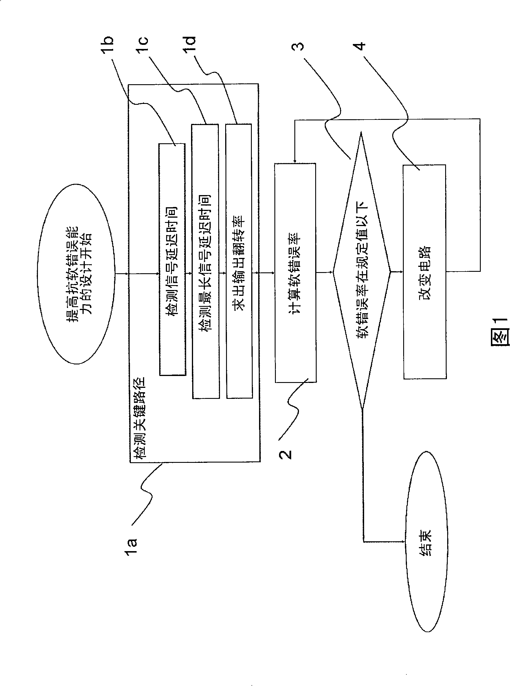
[0110] FIG. 1 is a flow chart showing a method of designing a semiconductor device with improved resistance to soft errors. Moreover, Fig. 1A shows: the process 1a of detecting the critical path; the process 1b of calculating the signal delay time; the process 1c of detecting the longest signal delay time; the process 1d of calculating the output turnover rate; the process 2 of calculating the soft error rate; Step 3 of judging whether the soft error rate is below a predetermined value; and step 4 of modifying the LSI circuit in order to reduce the soft error rate.

[0111] The step 1a of detecting a critical path is roughly as follows. In addition, the Example is demonstrated in detail using FIG. 2 later. First, the vas...

no. 2 example

[0169] The second embodiment relates to a signal transmission circuit having a structure that adjusts the delay time of signal transmission from a flip-flop on one side to a flip-flop on the other side, and represents an example of a signal transmission circuit that Using the above structure, the transmission circuit is modified to have the same delay time Td as the signal transmission circuit that has been determined as the critical path. 8A to 8D, 9A to 9D, 10A, and 10B, the signal transmission circuit of the second embodiment will be described. Moreover, Fig. 8A to Fig. 8D, Fig. 9A to Fig. 9D, Fig. 10A and Fig. 10B show, flip-flop 90, inverter 91, capacitor 92, capacitor 93, resistor 94, flip-flop circuit diagram 95, inverter circuit diagram 96. Dummy circuit diagram 97, capacitance pattern 99, capacitance pattern 100, resistance pattern 101, wiring pattern 102, groove pattern 103, field effect region pattern 104, gate pattern 105, and inverter 106 with low driving capabili...

no. 3 example

[0186] The third embodiment is an example of modifying the main flip-flop circuit of the flip-flop in the signal transmission circuit to a circuit having a low logic inversion rate of the held signal when noise is generated due to α line or the like. Furthermore, a third embodiment will be described using FIG. 11 .

[0187] FIG. 11 is a diagram showing a circuit of a flip-flop of a signal transmission circuit of a third embodiment having a main flip-flop having a low logic inversion rate of a signal held. 11 shows, clock signal 110, input signal 111, inverter 112, pass transistor 113, high voltage power supply (Vcc) 114, P-type transistors 115, 116, low-voltage power supply (Vss) 117, N-type Transistors 118 , 119 , inverters 120 , 121 , pass-gate transistor 122 , inverters 123 , 124 and output signal 125 .

[0188] The inverter 120 and the inverter 121 constitute a master flip-flop. The inverter 123 and the inverter 124 constitute a slave flip-flop. When the transmission ga...


PUM


Abstract

Provided is a semiconductor circuit device in which soft error resistance is enhanced while assuring the high-speed operation of an entire LSI circuit. A CAD device includes: means for identifying a signal transmission time of each signal transmission circuit of the LSI circuit; means for identifying an output inversion ratio upon radiation exposure of a flip-flop circuit of each signal transmission circuit; means for identifying a signal transmission circuit as a critical path; means for calculating a soft error ratio of the entire LSI circuit according to the signal transmission time, the output inversion ratio, and the clock cycle; and means for lowing the soft error ratio of the entire LSI circuit without changing the signal transmission time of the signal transmission circuit as the critical path when a predetermined soft error ratio is lower than the soft error ratio of the entire LSI circuit.

Description

technical field [0001] The present invention relates to a signal transmission circuit with improved resistance to soft errors, a semiconductor device including the signal transmission circuit, a design method for the semiconductor circuit device with improved resistance to soft errors, and a CAD (computer aided design) for realizing the design method : computer-aided design) device. Background technique [0002] It is known that α-rays, neutron rays from cosmic rays, etc., generated when radioactive isotopes contained in LSI (Large Scale Integration: Large Scale Integration) packages and wiring, etc., decay Electric noise is generated in the semiconductor circuit of the LSI, causing the semiconductor circuit to malfunction. The above-mentioned erroneous operation is called a soft error (soft error) as opposed to a hard error (hard error) caused by a failure of hardware such as a semiconductor circuit. Furthermore, for DRAM (dynamic random memory; dynamic random access memo...

Claims


Application Information

Patent Timeline
Patent Type & Authority Applications(China)
IPC IPC(8): G06F17/50H03K3/037H03K19/003H01L21/82
CPCG06F17/5045H03K3/0375H01L27/0207G06F30/30
Inventor 上村大树户坂义春
Owner SOCIONEXT INC
Why Eureka
Try Eureka