Design method of the semiconductor circuit device and CAD device
A computer-aided, circuit device technology, applied in computer-aided design, semiconductor device, semiconductor/solid-state device manufacturing, etc., to achieve the effect of improving resistance to soft errors without degrading overall performance
- Summary
- Abstract
- Description
- Claims
- Application Information
AI Technical Summary
Problems solved by technology
Method used
Image

Examples
no. 1 example
[0110] The first embodiment relates to a design method of a semiconductor device that improves resistance to soft errors. use figure 1 , Figure 2A to Figure 2C , Figure 3A to Figure 3C , Figure 4A , Figure 4B , Figure 5A to Figure 5C , Figure 6A , Figure 6B and Figure 7A to Figure 7C , to illustrate the design method of the above-mentioned semiconductor device.
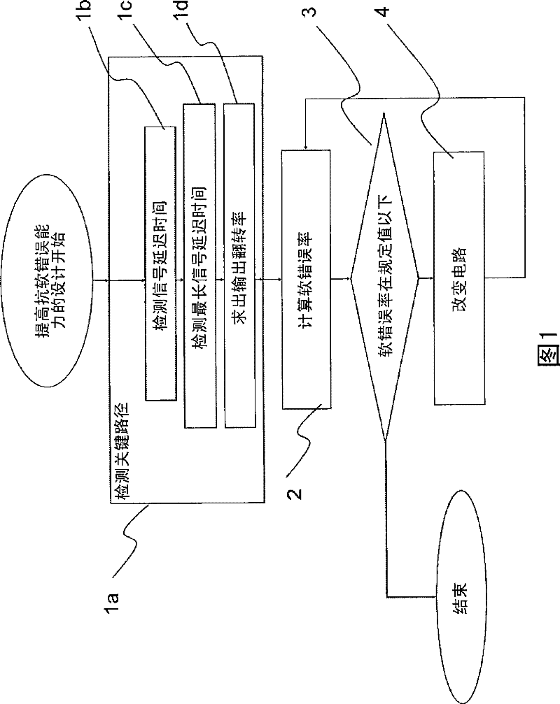
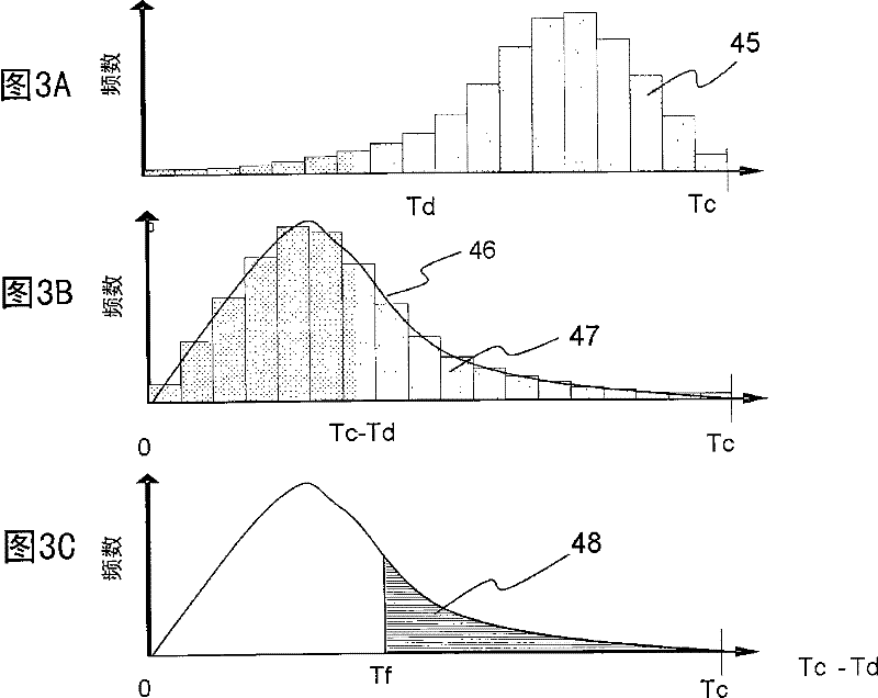
[0111] figure 1 It is a flowchart showing a design method of a semiconductor device with improved resistance to soft errors. and, figure 1 A means: process 1a of detecting critical path; process 1b of calculating signal delay time; process 1c of detecting longest signal delay time; process 1d of calculating output flip rate; process 2 of calculating soft error rate; judging soft error Step 3 of whether the rate is below the specified value; and Step 4 of modifying the LSI circuit in order to reduce the soft error rate.
[0112] The step 1a of detecting a critical path is roughly as follows. In ...
no. 2 example
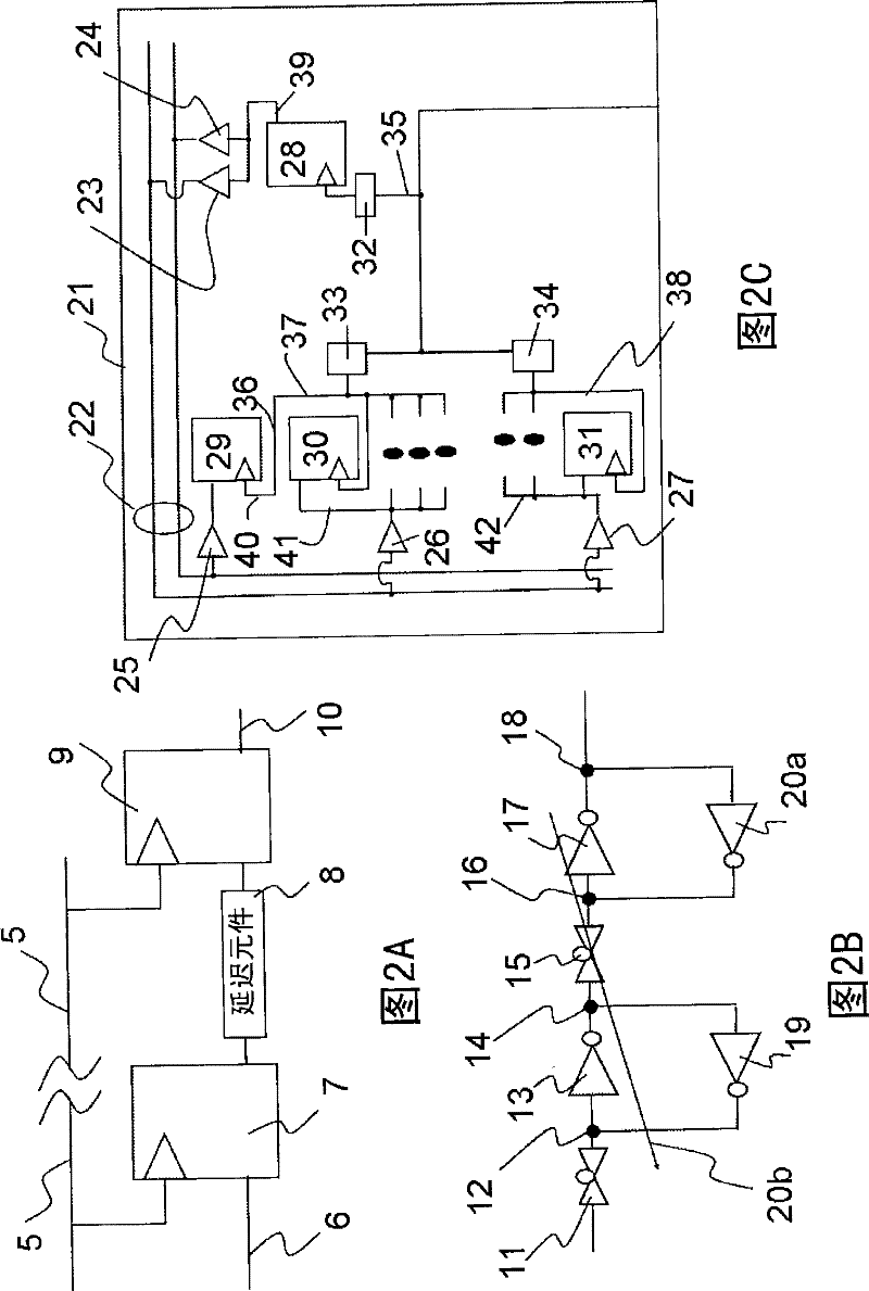
[0171] The second embodiment relates to a signal transmission circuit having a structure that adjusts the delay time of signal transmission from a flip-flop on one side to a flip-flop on the other side, and represents an example of a signal transmission circuit that Using the above structure, the transmission circuit is modified to have the same delay time Td as the signal transmission circuit that has been determined as the critical path. Also, take advantage of Figure 8A to Figure 8D , Figure 9A to Figure 9D , Figure 10A as well as Figure 10B , to describe the signal transmission circuit of the second embodiment. and, Figure 8A to Figure 8D , Figure 9A to Figure 9D , Figure 10A as well as Figure 10B Shown are flip-flop 90, inverter 91, capacitor 92, capacitor 93, resistor 94, flip-flop circuit diagram 95, inverter circuit diagram 96, dummy circuit diagram 97, capacitor pattern 99, capacitor pattern 100, resistor pattern 101, wiring Pattern 102, groove pattern...
no. 3 example
[0188] The third embodiment is an example of modifying the main flip-flop circuit of the flip-flop in the signal transmission circuit to a circuit having a low logic inversion rate of the held signal when noise is generated due to α line or the like. Also, take advantage of Figure 11 The third embodiment will be described.
[0189] Figure 11 It is a diagram showing a circuit of a flip-flop of the signal transmission circuit of the third embodiment having a main flip-flop having a low logic inversion rate of a signal held. and, Figure 11 Shown are clock signal 110, input signal 111, inverter 112, pass transistor 113, high voltage power supply (Vcc) 114, P-type transistors 115, 116, low voltage power supply (Vss) 117, N-type transistors 118, 119 , inverters 120 , 121 , transfer gate transistor 122 , inverters 123 , 124 and output signal 125 .
[0190] The inverter 120 and the inverter 121 constitute a master flip-flop. The inverter 123 and the inverter 124 constitute a s...
PUM
 Abstract
Description
Claims
Application Information
 - R&D
- Intellectual Property
- Life Sciences
- Materials
- Tech Scout
- Unparalleled Data Quality
- Higher Quality Content
- 60% Fewer Hallucinations
Browse by: Latest US Patents, China's latest patents, Technical Efficacy Thesaurus, Application Domain, Technology Topic, Popular Technical Reports.
© 2025 PatSnap. All rights reserved.Legal|Privacy policy|Modern Slavery Act Transparency Statement|Sitemap|About US| Contact US: help@patsnap.com