Array substrate, manufacturing method thereof, and display device

A technology of an array substrate and a manufacturing method, which is applied in the manufacturing of semiconductor/solid-state devices, semiconductor/solid-state device components, semiconductor devices, etc., can solve the problems of large depth, uneven surface of signal connection structure, abnormal connection, etc., to ensure display The effect of reducing the defect of falling off and avoiding the abnormal connection

Active Publication Date: 2021-11-09
BOE TECH GRP CO LTD
View PDF5 Cites 0 Cited by
  • Summary
  • Abstract
  • Description
  • Claims
  • Application Information

AI Technical Summary

Problems solved by technology

[0004] At present, there are two ways to fill the holes with metal. One is the sputtering method, that is, after the through-hole is made, a signal connection structure connecting the front and back of the display substrate is formed in the through-hole by sputtering. The substrate is thicker, the slope angle of the through hole is small, and the depth is large, which leads to the signal connection structure is prone to open circuit, and then abnormal connection occurs, which affects the display effect of the display product; the other is the electroplating method, that is, after the through hole is made, through The signal connection structure connecting the front and back of the display substrate is formed in the through hole, but after the signal connection structure is formed by electroplating, the surface of the signal connection structure is uneven. In order to carry out the subsequent IC (driver circuit) bonding (binding) process, it is necessary Planarize the surface of the signal connection structure, that is, use CMP (Chemical Mechanical Polishing) process to remove thick metal, but the adhesion between the metal and the substrate is poor, and the metal is easy to fall off during the CMP process, resulting in connection Abnormal, affecting the display effect of display products

Method used


Image

  • Array substrate, manufacturing method thereof, and display device
  • Array substrate, manufacturing method thereof, and display device
  • Array substrate, manufacturing method thereof, and display device

Examples


Embodiment 1

[0119] In this embodiment, the base substrate is a flexible substrate, and the manufacturing method of the array substrate specifically includes the following steps:

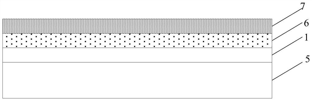
[0120] Step 1, such as image 3 As shown, a rigid carrier 5 is provided, a flexible substrate 1 is formed on the rigid carrier 5, and a first insulating layer 6 and a second insulating layer 7 are sequentially formed on the flexible substrate 1;

[0121] Wherein, the rigid carrier 5 can be a glass substrate or a quartz substrate; specifically, a layer of polyimide can be coated on the rigid carrier to form the flexible substrate 1 .

[0122] The etching rate of the second insulating layer 7 needs to be greater than the etching rate of the first insulating layer 6, and there is no limit to the materials used in the first insulating layer and the second insulating layer, as long as the insulation is satisfied and the etching rate of the second insulating layer 7 is greater than The etching rate of the first insul...

Embodiment 2

[0136] In this embodiment, the base substrate is a flexible substrate, and the manufacturing method of the array substrate specifically includes the following steps:

[0137] Step 1, such as Figure 10 As shown, a rigid carrier 5 is provided, a flexible substrate 1 is formed on the rigid carrier 5, and a negative photosensitive material layer 13 is formed on the flexible substrate 1;

[0138] Wherein, the rigid carrier 5 can be a glass substrate or a quartz substrate; specifically, a layer of polyimide can be coated on the rigid carrier to form the flexible substrate 1 .

[0139] Step 2, such as Figure 11 As shown, an electroplating seed layer 8 and a display unit 2 are formed on the negative photosensitive material layer 13, the electroplating seed layer 8 is connected to the signal input end of the display unit 2, and a protective film 3 covering the display unit 2 is formed;

[0140] Among them, the electroplating seed layer 8 is used for the subsequent electroplating pr...


PUM


Abstract

The invention provides an array substrate, a manufacturing method thereof, and a display device, belonging to the field of display technology. Wherein, the first side surface of the base substrate of the array substrate is provided with a display unit, and the second side surface is provided with a driving circuit, and the first side surface and the second side surface are the base substrate On the two opposite surfaces, the drive circuit is electrically connected to the display unit through a signal connection structure in at least one via hole structure, at least part of the via hole structure has a trapezoidal longitudinal section, and the trapezoid is close to the The base length of one side of the display unit is greater than the base length of the side of the trapezoid away from the display unit. Through the technical solution of the present invention, the display effect of the display device can be improved.

Description

technical field [0001] The present invention relates to the field of display technology, in particular to an array substrate, a manufacturing method thereof, and a display device. Background technique [0002] The display market is currently booming, and more new displays will emerge in the future as consumer demand continues to increase for a wide variety of display products such as laptops, smartphones, TVs, tablets, smart watches, and fitness wristbands product. [0003] At present, most of the display products have borders, and the connection terminals (such as the binding area of ​​the driving circuit) are usually arranged on the periphery of the display area of ​​the display panel. And full-screen borderless display products can enable users to obtain a better viewing experience, and will definitely detonate a new consumer market. Based on this, how to realize a display product with a full screen and no frame is a technical problem to be solved urgently by those skil...

Claims


Application Information

Patent Timeline
Patent Type & Authority Patents(China)
IPC IPC(8): H01L27/15H01L23/48H01L21/768
CPCH01L27/124H01L21/2885H01L21/76804H01L21/7684H01L21/76879H01L23/5226
Inventor 刘冬妮玄明花肖丽赵德涛陈亮陈昊
Owner BOE TECH GRP CO LTD
Why Eureka
Try Eureka