Inorganic perovskite thick-film composite semiconductor device and preparation method thereof

A composite material, inorganic calcium technology, used in semiconductor devices, electrical components, final product manufacturing, etc., can solve the problem that thin films cannot meet the physical needs of high-energy particle detection, do not have repeatability, and single crystals cannot be grown on a large scale or in large sizes, etc. question

Active Publication Date: 2021-05-07
SHANGHAI UNIV
View PDF4 Cites 0 Cited by
  • Summary
  • Abstract
  • Description
  • Claims
  • Application Information

AI Technical Summary

Problems solved by technology

CsPbBr is currently grown by temperature inversion 3 Single crystals are still unable to grow on a large scale and in large sizes, and are not repeatable
CbBr 3 Thin films of materials cannot meet the physical needs of high-energy particle detection

Method used


Image

  • Inorganic perovskite thick-film composite semiconductor device and preparation method thereof
  • Inorganic perovskite thick-film composite semiconductor device and preparation method thereof
  • Inorganic perovskite thick-film composite semiconductor device and preparation method thereof

Examples


Embodiment 1

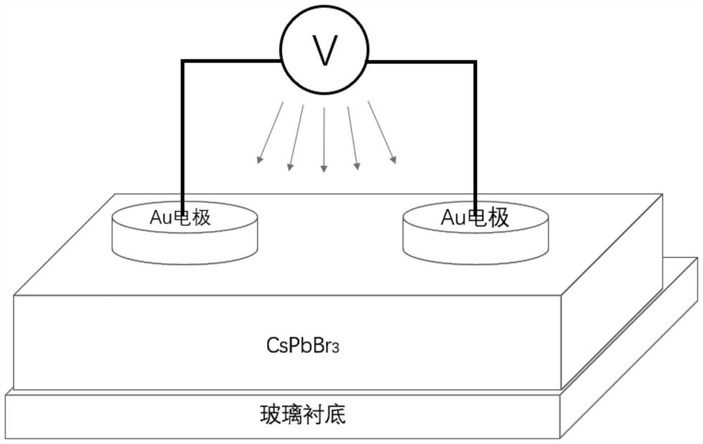
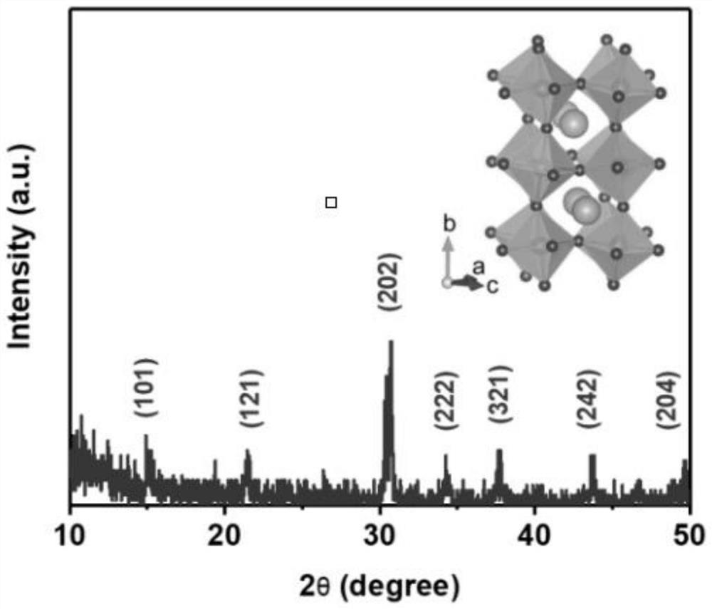
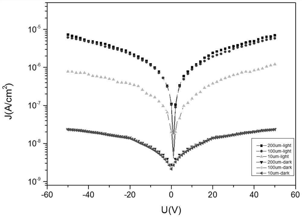
[0035] In this example, see figure 1 , an inorganic perovskite thick-film composite semiconductor device, the transparent glass is used as a substrate with a plane size of 2cm*2cm, and the inorganic perovskite thick-film composite semiconductor device consists of transparent glass, a perovskite light-absorbing layer, a metal The electrode is composed of transparent glass / CsPbBr 3 Composite structure composed of perovskite polycrystalline thick film / Au electrode as an all-inorganic perovskite planar semiconductor detector material, CsPbBr 3 Perovskite polycrystalline thick film as electron hole transport functional layer, CsPbBr 3 The thickness of the perovskite polycrystalline thick film is 10 μm, and the thickness of the Au electrode is 70 nm. The perovskite light-absorbing layer is prepared by a single-step thermal spraying method. The metal electrodes are composed of Au point electrodes. The inorganic perovskite thick-film composite device is used as an X-ray thick-film...

Embodiment 2

[0048] This embodiment is basically the same as Embodiment 1, especially in that:

[0049] In this embodiment, an inorganic perovskite thick-film composite semiconductor device, the transparent glass is used as a substrate with a planar size of 2cm*2cm, and the inorganic perovskite thick-film composite semiconductor device is made of transparent glass, perovskite Composed of mineral light-absorbing layer and metal electrodes, its structure is made of transparent glass / CsPbBr 3 Composite structure composed of perovskite polycrystalline thick film / Au electrode as an all-inorganic perovskite planar semiconductor detector material, CsPbBr 3 Perovskite polycrystalline thick film as electron hole transport functional layer, CsPbBr 3 The thickness of the perovskite polycrystalline thick film is 100 μm, and the thickness of the Au electrode is 80 nm. The perovskite light-absorbing layer is prepared by a single-step thermal spraying method. The metal electrodes are composed of Au po...

Embodiment 3

[0062] This embodiment is basically the same as the previous embodiment, and the special features are:

[0063] In this embodiment, an inorganic perovskite thick-film composite semiconductor device, the transparent glass is used as a substrate with a planar size of 2cm*2cm, and the inorganic perovskite thick-film composite semiconductor device is made of transparent glass, perovskite Composed of mineral light-absorbing layer and metal electrodes, its structure is made of transparent glass / CsPbBr 3Composite structure composed of perovskite polycrystalline thick film / Au electrode as an all-inorganic perovskite planar semiconductor detector material, CsPbBr 3 Perovskite polycrystalline thick film as electron hole transport functional layer, CsPbBr 3 The thickness of the perovskite polycrystalline thick film is 200 μm, and the thickness of the Au electrode is 90 nm. The perovskite light-absorbing layer is prepared by a single-step thermal spraying method. The metal electrodes a...


PUM

PropertyMeasurementUnit
thicknessaaaaaaaaaa
thicknessaaaaaaaaaa
thicknessaaaaaaaaaa

Abstract

The invention discloses an inorganic perovskite thick-film composite semiconductor device and a preparation method thereof, which can achieve continuous growth and prepare an X-ray detector with a large size and good crystallinity perovskite polycrystalline thick film , whose structure is transparent glass / CsPbBr 3 All-inorganic perovskite planar semiconductor detectors with perovskite polycrystalline thick film / Au electrodes. The detector we made is thicker, with higher on-off ratio, faster response speed and excellent water-oxygen stability. The preparation method of the semiconductor detector has simple steps, low cost, low temperature controllable process, and the prepared CsPbBr 3 The material has excellent moisture and heat resistance, and applying this method to large-scale commercial production has significant industrial promotion value.

Description

technical field [0001] The invention relates to a semiconductor detector device and a preparation process thereof, in particular to a perovskite thick-film compound semiconductor detector device and a preparation method thereof, which are applied in the technical field of semiconductor detector material manufacturing technology. Background technique [0002] Semiconductor detectors play a very important role in military or civilian fields such as biomedical sensing and high-energy particle detection. In recent years, halide perovskite materials have become a hot research material in the scientific research community due to their excellent photoelectric properties, suitable and easily adjustable bandgap, high carrier mobility, long carrier lifetime and low defect Such excellent characteristics make the perovskite semiconductor detector a new type of semiconductor detector with low cost and low temperature. The commonly used perovskite materials are mainly organic-inorganic h...

Claims


Application Information

Patent Timeline
Patent Type & Authority Patents(China)
IPC IPC(8): H01L31/08H01L31/0224H01L31/032H01L31/0368H01L31/18
CPCY02P70/50
Inventor 徐闰倪超伟欧正海张笑铮易永胜徐珊瑚徐飞黄健王林军
Owner SHANGHAI UNIV
Why Eureka
Try Eureka