Polysilicon ingot silicon wafer cleaning equipment

A silicon wafer cleaning and polysilicon technology, applied in electrical components, semiconductor/solid-state device manufacturing, circuits, etc., can solve the problems of low coordination between equipment, prolong processing time, and leave dead corners in polishing, and increase the polishing contact area. , Easy to operate, excellent structure

Active Publication Date: 2019-06-18
安徽华顺半导体发展有限公司
View PDF8 Cites 3 Cited by
  • Summary
  • Abstract
  • Description
  • Claims
  • Application Information

AI Technical Summary

Problems solved by technology

[0004] The object of the present invention is to provide a polysilicon ingot silicon wafer cleaning equipment to solve the traditional silicon wafer processing proposed in the above background technology. The cleaning equipment and the polishing equipment belong to two types of equipment, which are processed successively, prolonging the processing time. The matching degree is low, and during the polishing process, the position of the processing box is fixed, and the polishing will leave a dead angle, resulting in the problem of incomplete polishing

Method used


Image

  • Polysilicon ingot silicon wafer cleaning equipment
  • Polysilicon ingot silicon wafer cleaning equipment
  • Polysilicon ingot silicon wafer cleaning equipment

Examples


Embodiment Construction

[0019] The following will clearly and completely describe the technical solutions in the embodiments of the present invention with reference to the accompanying drawings in the embodiments of the present invention. Obviously, the described embodiments are only some, not all, embodiments of the present invention. Based on the embodiments of the present invention, all other embodiments obtained by persons of ordinary skill in the art without making creative efforts belong to the protection scope of the present invention.

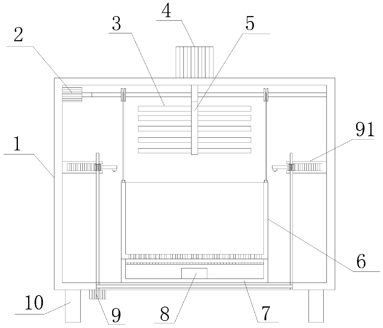
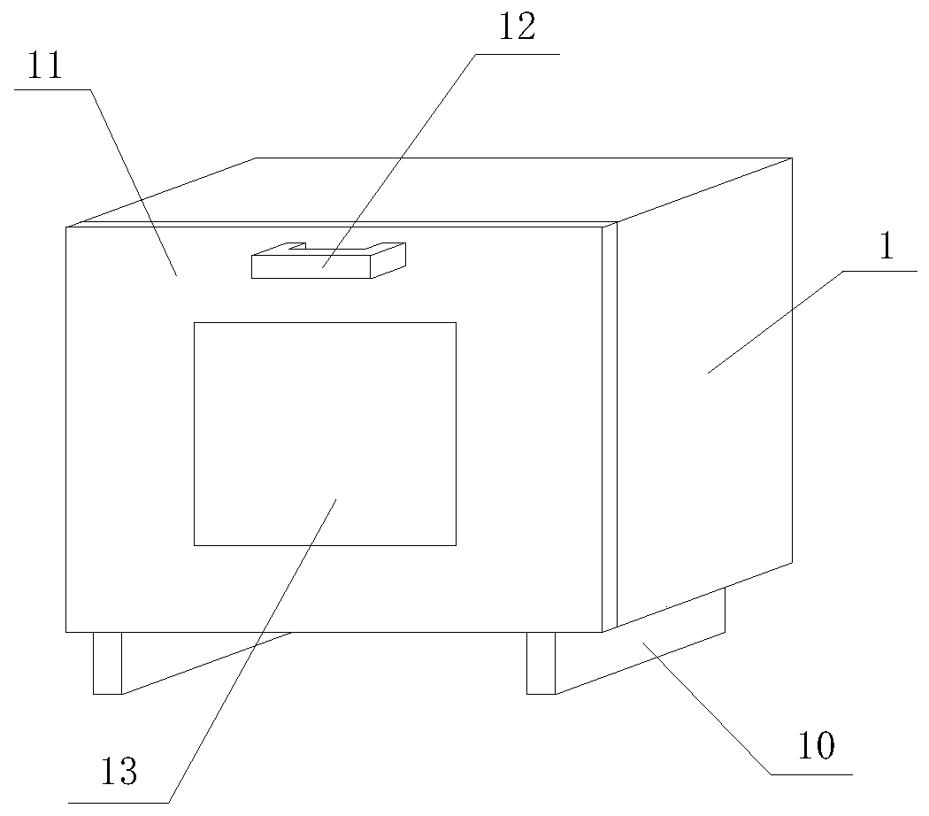
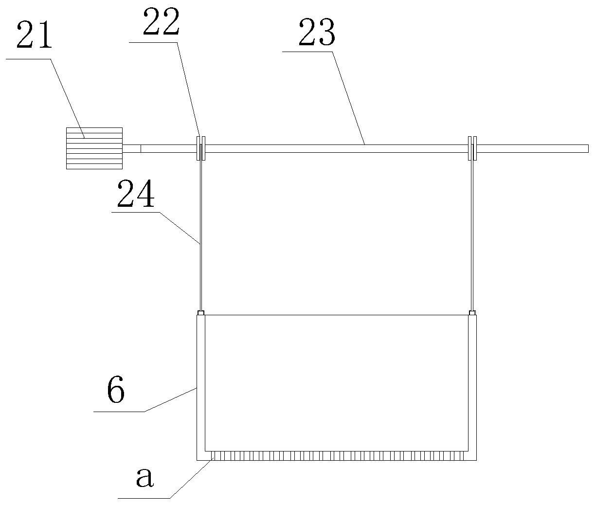
[0020] see Figure 1-4 , the present invention provides a technical solution: a polycrystalline silicon ingot silicon wafer cleaning equipment, including a device main body, a lifting mechanism 2 and a cleaning mechanism 9, the device main body includes a processing box 1, a polishing shaft 3, a driving machine 4, a rotating shaft 5, The inner box 6, the water collection tank 7, the pump body 8 and the legs 10, the legs 10 are arranged on the lower end surface...


PUM


Abstract

The invention relates to polysilicon ingot silicon wafer cleaning equipment. The polysilicon ingot silicon wafer cleaning equipment comprises a processing box body, polishing shafts, a driving machine, a rotating shaft, an inner box, a water collecting tank, a pump body, a first motor, two pulleys, a transmission shaft, ropes, a second motor, a bracket, a high-pressure spray head, a sliding block,a rack, a gear and an installation shaft, wherein the rotating shaft is rotationally connected into the processing box body and is in transmission connection with the output end of the driving machine; the polishing shafts are arranged on the rotating shaft; the inner box is positioned above the water collecting tank; the pulleys are symmetrically and rotationally connected to the transmission shaft and are fixedly connected with the inner box through the ropes; the transmission shaft is in transmission connection with the output end of the first motor; the rack is slidably connected into theprocessing box through the sliding block; the gear is rotationally connected into the processing box through the installation shaft; and the high-pressure spray head and the bronze-drum bracket are fixedly connected with the rack. The polysilicon ingot silicon wafer cleaning equipment is excellent in structure, reasonable in design, simple and convenient in operation, polishing dead corners are eliminated, polishing and cleaning two in one is achieved, and wide application prospect and high creativity are achieved.

Description

technical field [0001] The invention relates to the field of silicon wafer cleaning equipment, in particular to a polycrystalline silicon ingot silicon wafer cleaning equipment. Background technique [0002] Silicon wafers must be strictly cleaned in the production of semiconductor devices. Trace contamination can also lead to device failure. The purpose of cleaning is to remove surface contamination impurities, including organic and inorganic substances. Some of these impurities exist in the atomic state or ion state, and some exist in the form of thin films or particles on the surface of the silicon wafer. lead to various defects. There are two ways to remove pollution, physical cleaning and chemical cleaning. [0003] Physical cleaning is one of the cleaning methods. Physical cleaning often uses high-pressure nozzles to clean silicon wafers. However, in traditional silicon wafer processing, cleaning equipment and polishing equipment belong to two types of equipment. T...

Claims


Application Information

Patent Timeline
Patent Type & Authority Applications(China)
IPC IPC(8): H01L21/67
Inventor 李广森
Owner 安徽华顺半导体发展有限公司
Why Eureka
Try Eureka