Epitaxial wafer of light-emitting diode and preparation method of epitaxial wafer

A technology of light-emitting diodes and epitaxial wafers, applied in electrical components, circuits, semiconductor devices, etc., can solve the problems of unsatisfactory crystal quality and limited effect of epitaxial wafers

Active Publication Date: 2019-06-18
HC SEMITEK ZHEJIANG CO LTD
View PDF7 Cites 1 Cited by
  • Summary
  • Abstract
  • Description
  • Claims
  • Application Information

AI Technical Summary

Problems solved by technology

[0003] The setting of the AlN layer can relieve the large lattice mismatch between the substrate and the undoped GaN layer, so as to improve the overall crystal quality of the final epitaxial wafer, but the AlN layer relieves the large lattice mismatch between th

Method used


Image

  • Epitaxial wafer of light-emitting diode and preparation method of epitaxial wafer
  • Epitaxial wafer of light-emitting diode and preparation method of epitaxial wafer
  • Epitaxial wafer of light-emitting diode and preparation method of epitaxial wafer

Examples


Embodiment Construction

[0029] In order to make the objectives, technical solutions and advantages of the present invention clearer, the embodiments of the present invention will be further described in detail below with reference to the accompanying drawings.

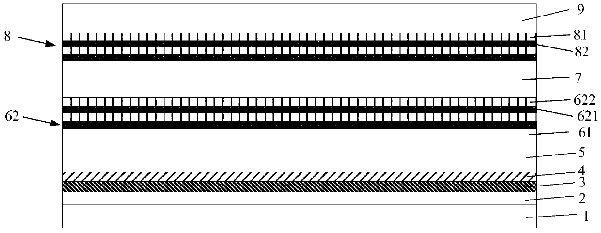
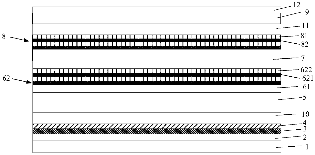
[0030] figure 1 It is a schematic structural diagram of a light-emitting diode epitaxial wafer provided by an embodiment of the present invention, as shown in figure 1As shown, the epitaxial wafer includes a substrate 1 and an AlN layer 2, Al x Ga 1-x N layer 3, Al y Ga 1.5y In 1-2.5y N layer 4 , undoped GaN layer 5 , stress release layer 6 , N-type GaN layer 7 , multiple quantum well layer 8 and P-type GaN layer 9 . Among them, 0.4≤x≤1, 0.2≤y≤0.4, Al x Ga 1-x The composition of Al in N layer 3 along the Al x Ga 1-x The growth direction of the N layer 3 gradually decreases, and the Al y Ga 1.5y In 1-2.5y The composition of Al in the N layer 4 along the Al y Ga 1.5y In 1-2.5y The growth direction of the N layer 4 gradually decre...


PUM

PropertyMeasurementUnit
Thicknessaaaaaaaaaa

Abstract

The invention discloses an epitaxial wafer of a light-emitting diode and a preparation method of the epitaxial wafer and belongs to the field of semiconductor optoelectronics. According to the method,an Al<x>Ga<1-x>N layer and an Al<y>Ga<1.5y>In<1-2.5y>N layer are sequentially arranged between an AlN layer and an undoped GaN layer, Al components in the Al<x>Ga<1-x>N layer and the Al<y>Ga<1.5y>In<1-2.5y>N layer can be within the ranges of 0.4<=x<=1 and 0.2<=y<=0.4, and when the Al components in the Al<x>Ga<1-x>N layer and the Al<y>Ga<1.5y>In<1-2.5y>N layer are within the ranges, lattice mismatch between the AlN layer and the undoped GaN layer can be relieved. Moreover, the Al component in the Al<x>Ga<1-x>N layer and the Al component in the Al<y>Ga<1.5y>In<1-2.5y>N layer are both graduallyreduced along the growing directions of the two layers, the Al components in the two layers are equal at the interface of the two layers, therefore, connection of the AlN layer and the undoped GaN layer can be well realized, defects generated due to lattice mismatch between the AlN layer and the undoped GaN layer are reduced, the crystal quality of the epitaxial wafer of the finally obtained light-emitting diode is improved, and the luminous efficiency of the finally obtained light-emitting diode is improved.

Description

technical field [0001] The invention relates to the field of semiconductor optoelectronics, in particular to an epitaxial wafer of a light emitting diode and a preparation method thereof. Background technique [0002] The epitaxial wafer is the basic structure for making light-emitting diodes. The structure of the epitaxial wafer includes a substrate and an epitaxial layer grown on the substrate. Wherein, the structure of the epitaxial layer mainly includes: an AlN layer, an undoped GaN layer, an N-type GaN layer, a multi-quantum well layer and a P-type GaN layer grown sequentially on the substrate. [0003] The setting of the AlN layer can relieve the large lattice mismatch between the substrate and the undoped GaN layer, so as to improve the overall crystal quality of the final epitaxial wafer, but the AlN layer relieves the large lattice mismatch between the substrate and the undoped GaN layer. The effect of the lattice mismatch between the layers is limited, so that the...

Claims


Application Information

Patent Timeline
IPC IPC(8): H01L33/02H01L33/12H01L33/00
Inventor 陶章峰程金连乔楠胡加辉李鹏
Owner HC SEMITEK ZHEJIANG CO LTD
Why Eureka
Try Eureka