
Variable gain amplifier and a continuous time linear equalizer

A technology of gain amplifier and linear equalizer, which is applied in the direction of gain control, amplification control, and improvement of control circuit by reducing distortion, etc. It can solve the problem that the voltage gain of variable gain amplifier is easily affected by power supply voltage, chip temperature, CMOS problems, etc.

Active Publication Date: 2019-06-18
PHOTONIC TECH SHANGHAI CO LTD
View PDF10 Cites 3 Cited by
  • Summary
  • Abstract
  • Description
  • Claims
  • Application Information

AI Technical Summary

Problems solved by technology

[0004] In view of the above-mentioned shortcoming of prior art, the purpose of the present invention is to provide a kind of variable gain amplifier and continuous time linear equalizer, for solving the voltage gain of existing variable gain amplifier is easily affected by power supply voltage, chip temperature, CMOS question

Method used


Image

  • Variable gain amplifier and a continuous time linear equalizer
  • Variable gain amplifier and a continuous time linear equalizer
  • Variable gain amplifier and a continuous time linear equalizer

Examples


Embodiment 1

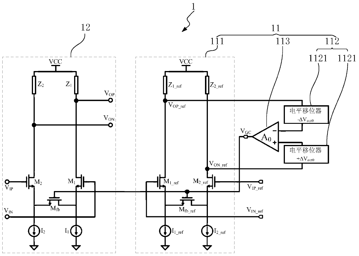
[0044] like figure 2 As shown, the present embodiment provides a variable gain amplifier, and the variable gain amplifier 1 includes:

[0045] The gain control voltage generation circuit 11 is used to input the reference voltage (V IN_ref , V IP_ref ) to generate the gain control voltage V GC ;

[0046] Signal path 12, connected to the gain control voltage generating circuit 11, for controlling the voltage V according to the gain GC Controlling the voltage gain of the signal path, realizes the differential input signal (V IN , V IP ) is differentially amplified to generate a differential output signal (V ON , V OP ).

[0047] As an example, such as figure 2 As shown, the gain control voltage generation circuit 11 includes:

[0048] The reference voltage signal path 111 is used for the differential input reference voltage (V IN_ref , V IP_ref ) is differentially amplified to generate a differential output reference voltage (V ON_ref , V OP_ref );

[0049] The l...

Embodiment 2

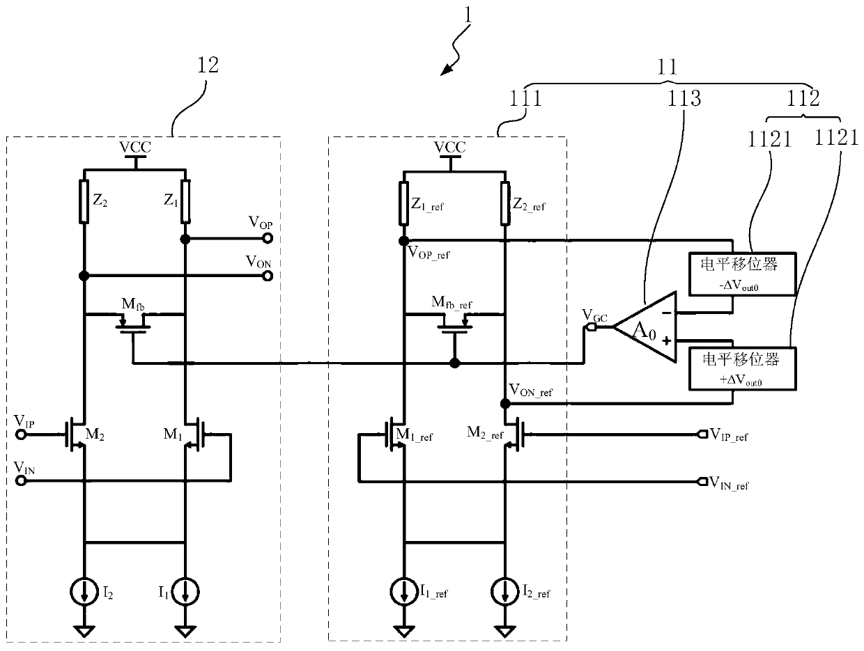
[0062] Such as image 3 As shown, the present embodiment provides a variable gain amplifier, and the variable gain amplifier 1 includes:

[0063] The gain control voltage generation circuit 11 is used to input the reference voltage (V IN_ref , V IP_ref ) to generate the gain control voltage V GC ;

[0064] Signal path 12, connected to the gain control voltage generating circuit 11, for controlling the voltage V according to the gain GC Controlling the voltage gain of the signal path 12 realizes the differential input signal (V IN , V IP ) is differentially amplified to generate a differential output signal (V ON , V OP ).

[0065] As an example, such as image 3 As shown, the gain control voltage generation circuit 11 includes:

[0066] The reference voltage signal path 111 is used for the differential input reference voltage (V IN_ref , V IP_ref ) is differentially amplified to generate a differential output reference voltage (V ON_ref , V OP_ref );

[0067] Th...

Embodiment 3

[0080] Such as Figure 4 As shown, the present embodiment provides a continuous time linear equalizer, and the continuous time linear equalizer 2 includes:

[0081] The high-frequency gain control voltage generation circuit 21 is used to input the high-frequency reference voltage (V IN_refH , V IP_refH ) to generate the high frequency gain control voltage V GC0 ;

[0082] The low-frequency gain control voltage generation circuit 22 is used to input the low-frequency reference voltage (V IN_refL , V IP_refL ) to generate the low frequency gain control voltage V GC1 ;

[0083] A signal path 23, connected to the high-frequency gain control voltage generation circuit 21 and the low-frequency gain control voltage generation circuit 22, for controlling the high-frequency gain voltage V according to the high-frequency gain control voltage V GC0 controlling the high frequency voltage gain of said signal path and controlling the voltage V according to said low frequency gain GC...


PUM


Abstract

The present invention provides a variable gain amplifier and a continuous time linear equalizer, the variable gain amplifier comprising: a gain control voltage generation circuit for generating a gaincontrol voltage according to a differential input reference voltage; and the signal pat connected to the gain control voltage generation circuit an used for controlling the voltage gain of the signalpath according to the gain control voltage and realizing differential amplification on the differential input signal according to the voltage gain to generate a differential output signal. Accordingto the variable gain amplifier, the problem that the voltage gain of an existing variable gain amplifier is easily subjected to power supply voltage, chip temperature and CMOS is solved.

Description

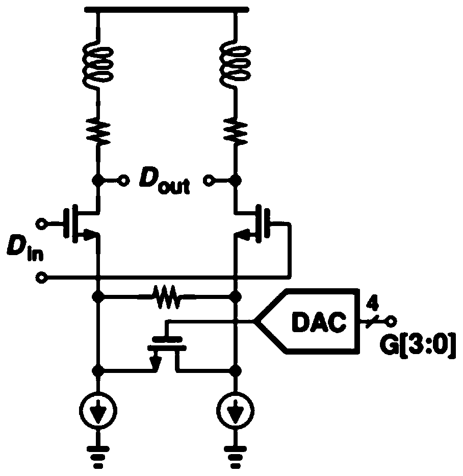
technical field [0001] The invention relates to the field of ultra-wideband communication integrated circuits, in particular to a variable gain amplifier and a continuous time linear equalizer. Background technique [0002] In high-speed ultra-wideband communication integrated circuits (such as high-speed serial transceiver system chips, high-speed serializer / deserializer chips, high-speed optical communication chips), variable gain amplifiers (VGA) and continuous time equalizers (CTLE) have the most Wide range of applications. Among them, the variable gain amplifier (VGA) is used in the analog front end of the receiver / transmitter of the communication circuit, which provides an adjustable gain within a certain range according to actual needs, and amplifies or attenuates the signal; and the continuous time equalizer (CTLE ) is mainly used in the signal receiving end of the communication circuit to compensate the high-frequency attenuation of the signal. [0003] figure 1 ...

Claims


Application Information

Patent Timeline
Patent Type & Authority Applications(China)
IPC IPC(8): H03G1/04H03G3/30
CPCY02D30/70
Inventor 夏韬白睿彭毅王心
Owner PHOTONIC TECH SHANGHAI CO LTD
Learn More