Memristive device based on transition metal carbide and preparation method thereof

A transition metal, memristive device technology, applied in electrical components and other directions, can solve problems such as poor synaptic plasticity effect, and achieve the effects of low cost, good conductivity and stability, and broad application prospects.

Inactive Publication Date: 2019-07-02
NANJING UNIV OF POSTS & TELECOMM
View PDF0 Cites 4 Cited by
  • Summary
  • Abstract
  • Description
  • Claims
  • Application Information

AI Technical Summary

Problems solved by technology

[0003] In the prior art, electrical tests, physical characterization and bioplasticity tests were performe

Method used


Image

  • Memristive device based on transition metal carbide and preparation method thereof
  • Memristive device based on transition metal carbide and preparation method thereof
  • Memristive device based on transition metal carbide and preparation method thereof

Examples


preparation example Construction

[0038] The present invention also provides a method for preparing the above-mentioned memristive device, comprising the following steps:

[0039] S1) Bottom electrode deposition: In a vacuum environment, the substrate is fixed on the target gun of the sputtering system, the bottom electrode material is selected as the sputtering source, and the bottom electrode is deposited by a magnetron sputtering device. The bottom electrode is evenly and completely covered on the substrate. bottom surface;

[0040] S2) Dielectric layer sputtering: maintain the vacuum environment in step S1, replace the dielectric layer sputtering source, and uniformly and completely sputter the dielectric layer on the upper surface of the bottom electrode;

[0041] S3) Preparation of transition metal carbide suspension: mix transition metal carbide and deionized water at a mass ratio of 1:150, stir for 5min-15min, and prepare transition metal carbide suspension;

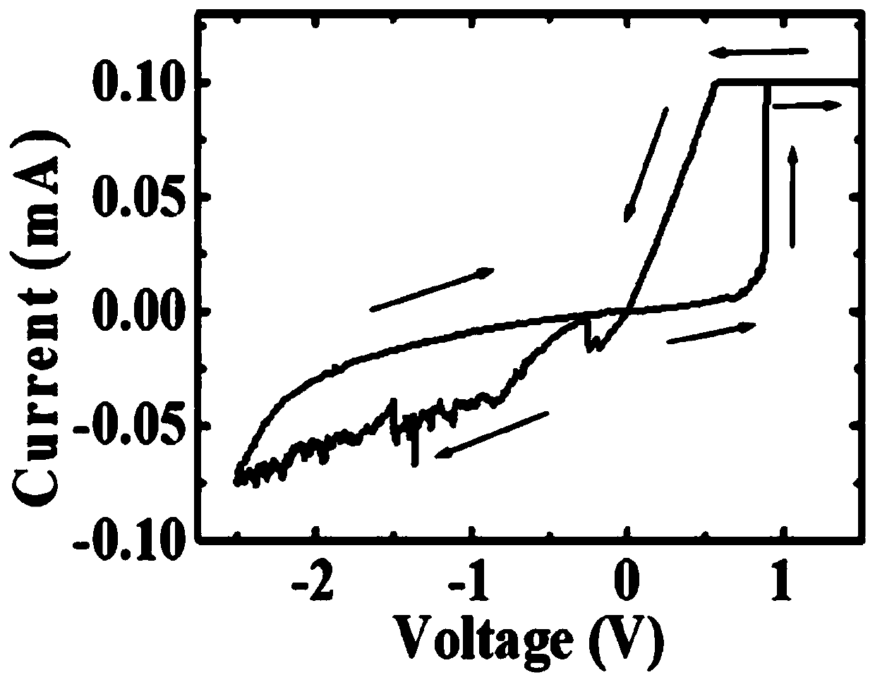
[0042] S4) Preparation of the resistive l...

Embodiment 1

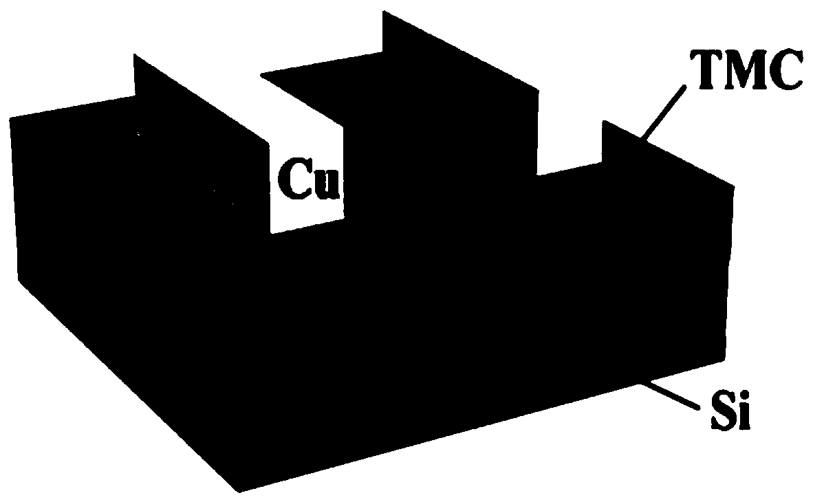
[0046]A memristive device with a structure of copper / transition metal carbide / silicon dioxide / tungsten, the preparation method of which comprises the following steps:

[0047] S1) In a vacuum environment, fix the silicon substrate on the target gun of the sputtering system, select tungsten as the sputtering source, and deposit a tungsten electrode with a thickness of 90 nm by magnetron sputtering. The tungsten electrode is evenly and completely covered on the silicon the upper surface of the substrate;

[0048] S2) Maintaining the vacuum environment in step S1, replacing the silicon dioxide sputtering source, uniformly and completely sputtering a silicon dioxide dielectric layer with a thickness of 80 nm on the upper surface of the tungsten electrode;

[0049] S3) Take the transition metal carbide and deionized water and mix according to the mass ratio of 1:100, and stir for 10 minutes to prepare the transition metal carbide suspension;

[0050] S4) Absorb the upper turbid li...


PUM

PropertyMeasurementUnit
Thicknessaaaaaaaaaa
Thicknessaaaaaaaaaa
Thicknessaaaaaaaaaa

Abstract

The invention provides a memristive device based on transition metal carbide. The memristive device comprises a top electrode, a resistive layer and a bottom electrode which are arranged in order fromtop to bottom, wherein the resistive layer and the bottom electrode match a substrate in shape and size; the resistive layer includes a dielectric layer and a transition metal carbide film disposed over the dielectric layer; the top electrode is sputtered on the top of the transition metal carbide film through the opening of a mask plate; and the top and the bottom of the bottom electrode are incontact with the dielectric layer and the substrate. The memristive device has good conductivity and stability, can simulate the change of synaptic weighting, realizes a function of simulating the synaptic plasticity, and has a broad application prospect. In addition, the preparation method of the invention is simple, efficient, and low in cost.

Description

technical field [0001] The invention relates to a memristive device and a preparation method thereof, in particular to a transition metal carbide-based memristive device and a preparation method thereof, belonging to the technical fields of brain-inspired devices, brain-inspired computing systems, and brain-inspired neural circuits. Background technique [0002] Brain-like computing, compared with traditional computing that relies on the von Neumann architecture, has shown strong advantages in various cognitive tasks. The memristive device is a two-port nonlinear passive electronic device based on the resistance transition effect, which can memorize the amount of charge flowing through it. It has characteristics very similar to neural synapses and can be used as the best choice for artificial synapses. Investigating the short-term plasticity of synapses simulated by memristive devices is crucial for the development of neuromorphic computing. [0003] In the prior art, elect...

Claims


Application Information

Patent Timeline
IPC IPC(8): H01L45/00
CPCH10N70/881H10N70/021H10N70/011
Inventor 童祎高斐渠开放沈心怡郭宇锋万相连晓娟
Owner NANJING UNIV OF POSTS & TELECOMM
Why Eureka
Try Eureka