Ordered nanostructure array-based LSPR sensing device
A nanostructure and sensing device technology, applied in the field of optical sensors, to achieve the effect of qualitative detection and simple structure
- Summary
- Abstract
- Description
- Claims
- Application Information
AI Technical Summary
Problems solved by technology
Method used
Image
Examples
Embodiment 1
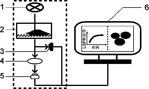
[0025] This embodiment provides an LSPR sensing device based on an ordered nanostructure array, including a light source unit 1 , a sensing unit 2 , a detection unit 3 and a display unit 6 . The sensing unit 2 is arranged between the light source unit 1 and the detection unit 3 , and the detection unit 3 is electrically connected to the display unit 6 . The light source unit 1 is used to provide light signals. The sensing unit 2 is a semi-closed cell culture tank with an ordered nanostructure array integrated on the inner surface, which facilitates the adhesion and spreading of cells on the surface of the ordered nanostructure array in the culture tank. The light signal emitted by the light source unit 1 can pass through the sensing unit 2 to reach the detection unit 3, and the detection unit 3 is used for converting the light signal into an electrical signal. The display unit 6 is used to output detection results, and is generally a terminal with data processing and display ...
Embodiment 2
[0029] Such as figure 1 , figure 2 and image 3 As shown, this embodiment is similar to Embodiment 1, and further, the LSPR sensing device also includes a topography observation unit 4 and a topography recording unit 5, and the topography observation unit 4 is used in the observation sensing unit 2 The shape of the cell, the shape recording unit 5 is used to record the shape of the cell and transmit the result to the display unit 6. In this embodiment, the morphology observation unit 4 is a microscope with an optical magnification function, which can enlarge the topography image of the cell surface to be visible to the naked eye; The inductive coupling element for converting images into electrical signals converts the optical microscopic images into electrical signals in real time and transmits them to the display unit 6 . In addition, the light source unit 1 in this embodiment is a monochromatic light source, that is, it can be used directly without being processed by a b...
Embodiment 3
[0035]This embodiment is similar to embodiment 1 or 2, the main difference is that the light source unit 1 is a light emitting diode with a center wavelength of 700 nm. In addition, the ordered nanostructure array integrated on the inner surface of the sensing unit 2 is a gold nanotriangular array, and the sensing unit 2 , shape observation unit 4 and shape recording unit 5 are arranged on the same side of the light source unit 1 .
PUM
| Property | Measurement | Unit |
|---|---|---|
| thickness | aaaaa | aaaaa |
| wavelength | aaaaa | aaaaa |
Abstract
Description
Claims
Application Information


