Manufacturing method for deep trough isolation structure

A technology of isolation structure and manufacturing method, used in semiconductor/solid-state device manufacturing, electrical components, circuits, etc., can solve the problems of low wafer yield, low photoresist etching rate, etc., to solve the problem of low yield and thickening Deposit thickness, avoid thermal process effects

Inactive Publication Date: 2019-07-09
SHANGHAI HUAHONG GRACE SEMICON MFG CORP
View PDF4 Cites 2 Cited by
  • Summary
  • Abstract
  • Description
  • Claims
  • Application Information

AI Technical Summary

Problems solved by technology

[0003] The purpose of the present invention is to provide a method for manufacturing a deep trench isolation structure to solve the problems of low photoresist etching rate and low wafer yield

Method used


Image

  • Manufacturing method for deep trough isolation structure
  • Manufacturing method for deep trough isolation structure
  • Manufacturing method for deep trough isolation structure

Examples


Embodiment Construction

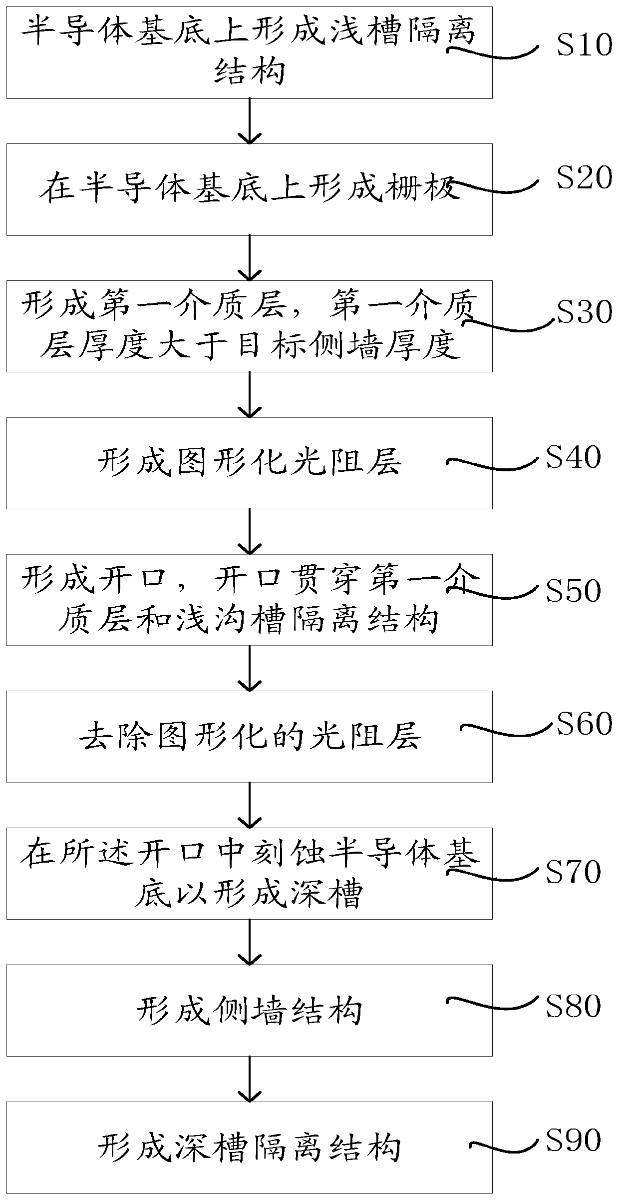
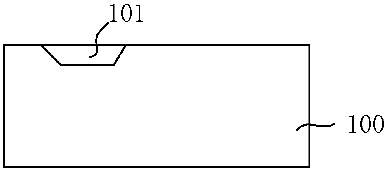
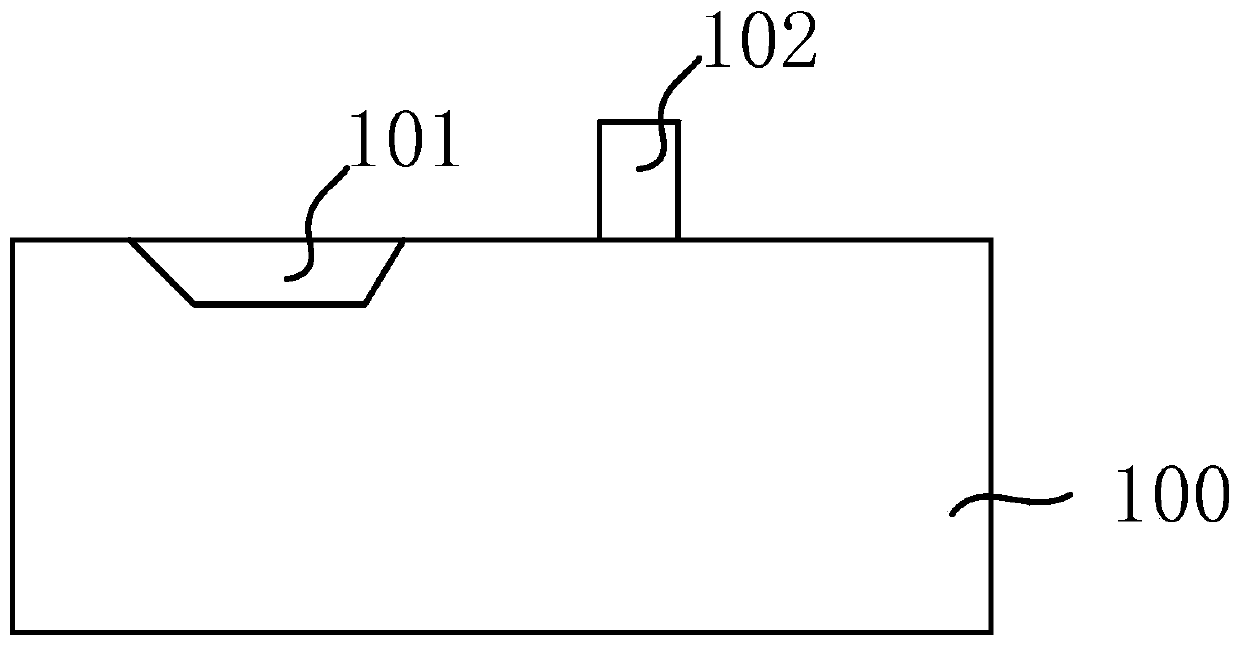
[0030] The manufacturing method of the deep trench isolation structure proposed by the present invention will be further described in detail below with reference to the accompanying drawings and specific embodiments. Advantages and features of the present invention will be apparent from the following description and claims. It should be noted that all the drawings are in a very simplified form and use imprecise scales, and are only used to facilitate and clearly assist the purpose of illustrating the embodiments of the present invention. In addition, the structures shown in the drawings are often a part of the actual structure. In particular, each drawing needs to display different emphases, and sometimes uses different scales.

[0031] Please refer to Figure 1-Figure 10 , figure 1 is a flowchart of a method for manufacturing a deep trench isolation structure according to an embodiment of the present invention; Figure 2-Figure 10 It is a structural schematic diagram of e...


PUM

PropertyMeasurementUnit
thicknessaaaaaaaaaa

Abstract

The invention provides a manufacturing method for a deep trough isolation structure. The manufacturing method is characterized in that a semiconductor substrate is provided, a shallow trough isolationstructure and a grid are formed in the semiconductor substrate; a first dielectric layer is formed, the first dielectric layer covers the semiconductor substrate, the shallow trough isolation structure and the grid, and thickness of the first dielectric layer is greater than thickness of a target side; an opening is formed, the opening penetrates through the first dielectric layer and the shallowtrough isolation structure, and the semiconductor substrate is exposed; the first dielectric layer is taken as a mask, and the semiconductor substrate is etched in the opening to form a deep trough;the first dielectric layer on the surface of the semiconductor substrate, the surface of the shallow trough isolation structure and a top surface of the grid is removed, the first dielectric layer ona side wall of the grid is reserved to form a side wall structure, and thickness of the side wall structure is thickness of the target side wall; a second dielectric layer is formed, and the deep trough is filled by the second dielectric layer to form the deep trough isolation structure.

Description

technical field [0001] The invention relates to the technical field of semiconductors, in particular to a method for manufacturing a deep trench isolation structure. Background technique [0002] In the existing semiconductor manufacturing technology, the deep trench isolation structure is generally formed after the gate and sidewalls are formed, and after the deep trench photolithography, the photoresist layer is used to stop the deep trench etching, and then the interlayer dielectric is used to fill it together. Chemical mechanical planarization, this method takes a long time to etch deep grooves, consumes a lot of photoresist, and forms a large amount of polymers, which leads to a decrease in the etching rate in the grooves, and also forms lumps and falls to the crystal after gathering at the top of the grooves. Affects the yield on the circle. Contents of the invention [0003] The object of the present invention is to provide a method for manufacturing a deep trench ...

Claims


Application Information

Patent Timeline
Patent Type & Authority Applications(China)
IPC IPC(8): H01L21/762
CPCH01L21/76224
Inventor 蒙飞
Owner SHANGHAI HUAHONG GRACE SEMICON MFG CORP
Why Eureka
Try Eureka