Semiconductor device and forming method thereof

A semiconductor and device technology, applied in the field of semiconductor devices and their formation, can solve problems such as performance to be improved, and achieve the effects of optimizing performance, reducing power, and improving performance

Active Publication Date: 2019-07-09
SEMICON MFG INT (SHANGHAI) CORP +1
View PDF5 Cites 0 Cited by
  • Summary
  • Abstract
  • Description
  • Claims
  • Application Information

AI Technical Summary

Problems solved by technology

[0004] However, the performance of semiconductor devices composed of fin field effect transistors in the prior art still needs to be improved

Method used


Image

  • Semiconductor device and forming method thereof
  • Semiconductor device and forming method thereof
  • Semiconductor device and forming method thereof

Examples


Embodiment Construction

[0028] As mentioned in the background, semiconductor devices formed in the prior art have poor performance.

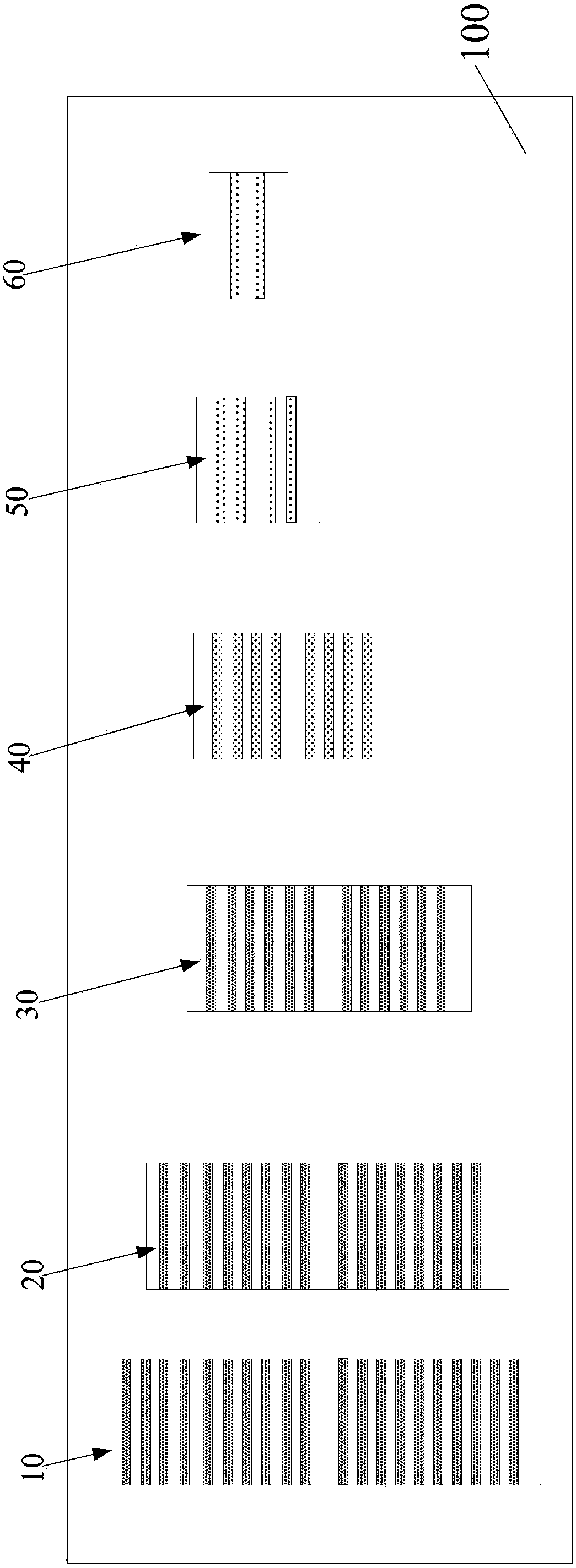
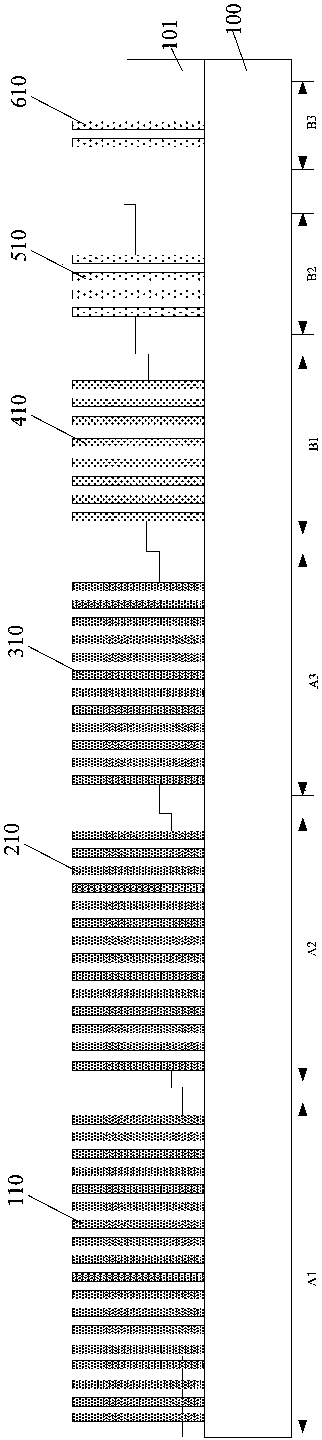
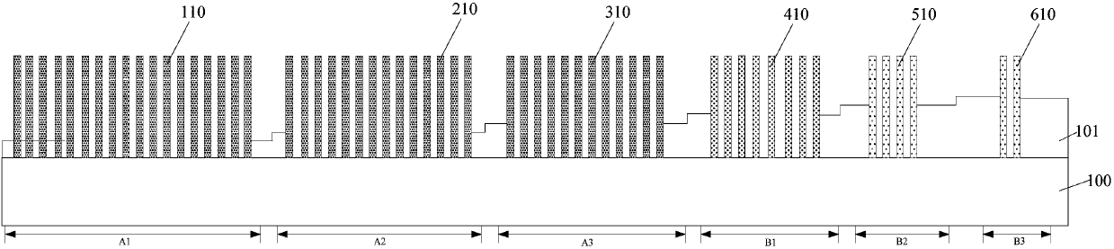
[0029] A semiconductor device, comprising: a semiconductor substrate, a first chip area and a second chip area separated from each other on the semiconductor substrate; a first logic standard cell located on the first chip area; a second chip area located on the second chip area Two logic standard cells; the first logic standard cell has a first cell height, the second logic standard cell has a second cell height, and the first cell height is greater than the second cell height; the first logic standard cell has a first operating frequency and a first Power consumption, the second logic standard cell has a second operating frequency and second power consumption, the first operating frequency is greater than the second operating frequency, the first power consumption is greater than the second power consumption; the first logic standard cell includes The first fin on th...


PUM


Abstract

Disclosed are a semiconductor device and a forming method thereof. The semiconductor device comprises a semiconductor substrate, a high-frequency type logic standard unit and a low-power-consumption type logic standard unit, wherein the semiconductor substrate comprises a high-frequency region set and a low-power-consumption region set; the high-frequency type logic standard unit is located on thehigh-frequency region set, wherein the high-frequency type logic standard unit has high-frequency type unit height, high-frequency type working frequency and high-frequency type power; the low-power-consumption type logic standard unit is located on the low-power-consumption region set, and the low-power-consumption type logic standard unit has low-power-consumption type unit height, low-power-consumption type working frequency and low-power-consumption type power; the high-frequency type unit height is larger than the low-power-consumption type unit height; the high-frequency type working frequency is greater than the low-frequency type working frequency; the high-frequency type power is greater than the low-frequency type power; the high-frequency type logic standard unit comprises a high-frequency type fin part; the low-power-consumption type logic standard unit comprises a low-power-consumption type fin part; and the effective height of the high-frequency type fin part is larger than that of the low-power-consumption type fin part. The performance of the semiconductor device is improved.

Description

technical field [0001] The invention relates to the field of semiconductor manufacturing, in particular to a semiconductor device and a forming method thereof. Background technique [0002] MOS (Metal-Oxide-Semiconductor) transistors are one of the most important components in modern integrated circuits. The basic structure of the MOS transistor includes: a semiconductor substrate; a gate structure located on the surface of the semiconductor substrate, and the gate structure includes: a gate dielectric layer located on the surface of the semiconductor substrate and a gate electrode layer located on the surface of the gate dielectric layer; The source and drain doped regions in the semiconductor substrate on both sides of the pole structure. [0003] With the development of semiconductor technology, the ability of the traditional planar MOS transistor to control the channel current becomes weaker, resulting in serious leakage current. Fin Field Effect Transistor (Fin FET) i...

Claims


Application Information

Patent Timeline
Patent Type & Authority Applications(China)
IPC IPC(8): H01L27/088H01L21/8234
CPCH01L27/0886H01L21/823431H01L21/762H01L29/785H01L27/0207H01L27/11807H01L29/66795H01L21/31116H01L27/105H01L21/3105
Inventor 张欣贵董耀旗
Owner SEMICON MFG INT (SHANGHAI) CORP
Why Eureka
Try Eureka