QLED device and preparation method thereof
A device and magnetic material technology, applied in the field of quantum dots, can solve the problems of carrier injection imbalance, affecting device luminous efficiency and stability, etc., to improve injection balance, improve luminous efficiency and stability, and the process is simple and easy Effect
- Summary
- Abstract
- Description
- Claims
- Application Information
AI Technical Summary
Problems solved by technology
Method used
Image

Examples
preparation example Construction
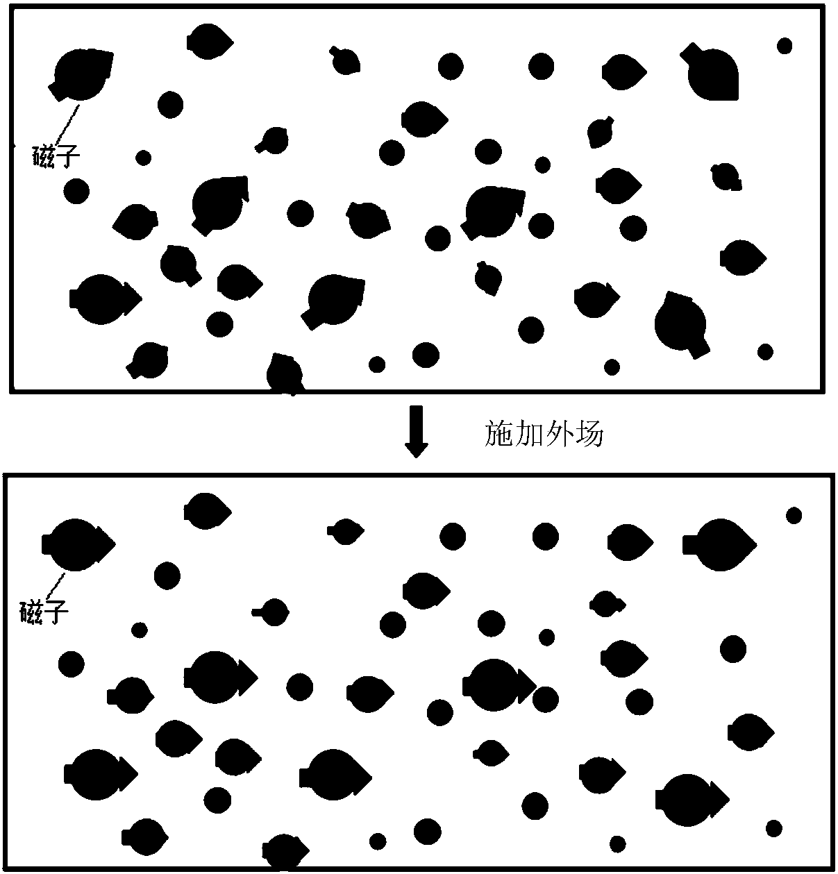
[0034] When the magnetic layer is used as a magnetic layer at the interface of each functional layer of the device, it can be placed between HIL (hole injection layer) and HTL (hole transport layer), between HTL and EML (quantum dot light emitting layer), between EML and ETL Between the (electron transport layer), between the EIL (electron injection layer) and the ETL, and between the electrode and the HIL / EIL, may be a single-layer structure or a multi-layer structure. The selection of magnetic layer materials includes but not limited to conductive magnetic materials and insulating magnetic materials, conductive magnetic materials such as Fe, Co, Ni and other transition group metals and their alloys, and oxides thereof, insulating magnetic materials such as sintered ferrite, magnetic rubber etc. Furthermore, for conductive magnetic materials, the thickness of the magnetic layer is controlled at 1nm-10nm. When the thickness of the magnetic layer of the conductive magnetic mate...
Embodiment 1
[0057] A magnetic layer made of a magnetic material is disposed between the quantum dot light emitting layer and the electron transport layer of the QLED device.
[0058] The QLED device structure is: ITO / PEDOT:PSS / Poly-TPD / PVK / Green QDs / MagneticLayer / ZnO / Al. The preparation method of the QLED device is as follows: first spin-coat PEDOT:PSS on the glass substrate containing the ITO electrode at a rotation speed of 5000r.p.m. for 30s, then heat at 120°C in the air for 20min, and control the thickness at about 35nm. Spin-coat 1wt% Poly-TPD dissolved in chlorobenzene at a rotation speed of 2500r.p.m. for 30s, then heat at 110°C for 30min in nitrogen, and control the thickness at about 30nm. Spin-coat 2mg / ml PVK dissolved in toluene at a speed of 2500r.p.m. for 30s, and control the thickness at about 5nm. Then spin-coat 30mg / ml CdSe-CdS core-shell quantum dots dissolved in toluene at a rotation speed of 800r.p.m. for 30s, then heat at 120°C for 15min in nitrogen, and control the ...
Embodiment 2
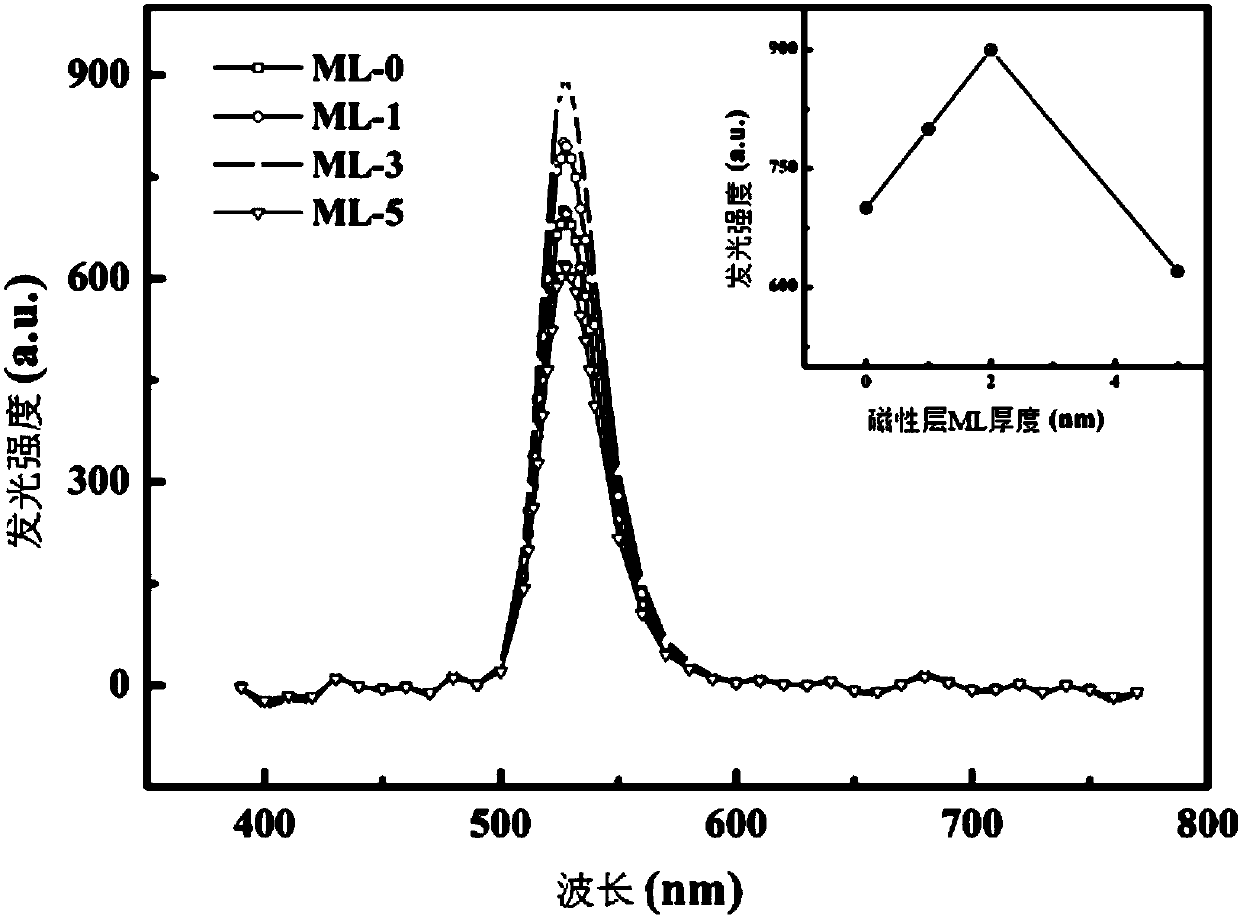
[0061] A magnetic layer made of magnetic material is arranged between the quantum dot light-emitting layer and the hole transport layer of the QLED device.
[0062] The QLED device structure is ITO / PEDOT:PSS / Poly-TPD / PVK / Magnetic Layer / GreenQDs / ZnO / Al. The preparation method of each layer of the QLED device is similar to the above-mentioned Example 1, the thickness of the ML layer is also controlled at 0nm, 1nm, 3nm, and 5nm, and the brightness of the device is 8000cd / m at a current of 2mA. 2 、10564cd / m 2 、6000cd / m 2 、4000cd / m 2 . It can be seen that when the ML thickness is 1 nm, the performance of the device is relatively good, and the brightness is increased by 32% compared with that without ML.
PUM
 Abstract
Description
Claims
Application Information
 - R&D
- Intellectual Property
- Life Sciences
- Materials
- Tech Scout
- Unparalleled Data Quality
- Higher Quality Content
- 60% Fewer Hallucinations
Browse by: Latest US Patents, China's latest patents, Technical Efficacy Thesaurus, Application Domain, Technology Topic, Popular Technical Reports.
© 2025 PatSnap. All rights reserved.Legal|Privacy policy|Modern Slavery Act Transparency Statement|Sitemap|About US| Contact US: help@patsnap.com