
Electrode and QLED device

A technology of electrodes and electrode materials, applied in the field of quantum dots, can solve problems such as carrier injection imbalance, affecting device luminous efficiency and stability, and achieve the effect of improving injection balance, luminous efficiency and stability

Active Publication Date: 2019-07-09
TCL CORPORATION
View PDF5 Cites 2 Cited by
  • Summary
  • Abstract
  • Description
  • Claims
  • Application Information

AI Technical Summary

Problems solved by technology

[0004] The purpose of the present invention is to overcome the above-mentioned deficiencies of the prior art, and provide an electrode and a QLED device, aiming at solving the technical problem of unbalanced carrier injection in the existing QLED device, thereby affecting the luminous efficiency and stability of the device

Method used


Image

  • Electrode and QLED device
  • Electrode and QLED device
  • Electrode and QLED device

Examples


preparation example Construction

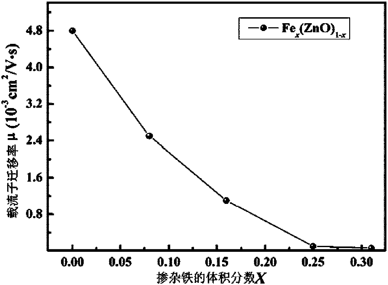
[0032] When the magnetic layer is used as a magnetic layer at the interface of each functional layer of the device, it can be placed between HIL (hole injection layer) and HTL (hole transport layer), between HTL and EML (quantum dot light emitting layer), between EML and ETL Between the (electron transport layer), between the EIL (electron injection layer) and the ETL, and between the electrode and the HIL / EIL, may be a single-layer structure or a multi-layer structure. The selection of magnetic layer materials includes but not limited to conductive magnetic materials and insulating magnetic materials, conductive magnetic materials such as Fe, Co, Ni and other transition group metals and their alloys, and oxides thereof, insulating magnetic materials such as sintered ferrite, magnetic rubber etc. Furthermore, for conductive magnetic materials, the thickness of the magnetic layer is controlled at 1nm-10nm. When the thickness of the magnetic layer of the conductive magnetic mate...

Embodiment 1

[0055] A magnetic layer made of a magnetic material is disposed between the quantum dot light emitting layer and the electron transport layer of the QLED device.

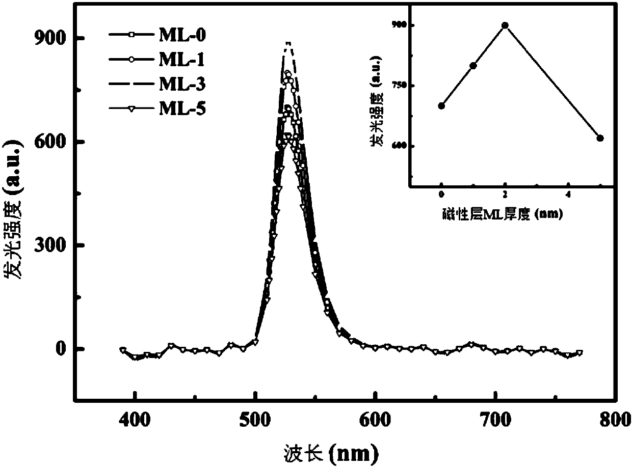
[0056] The QLED device structure is: ITO / PEDOT:PSS / Poly-TPD / PVK / Green QDs / Magnetic Layer / ZnO / Al. The preparation method of the QLED device is as follows: first spin-coat PEDOT:PSS on the glass substrate containing the ITO electrode at a rotation speed of 5000r.p.m. for 30s, then heat at 120°C in the air for 20min, and control the thickness at about 35nm. Spin-coat 1wt% Poly-TPD dissolved in chlorobenzene at a rotation speed of 2500r.p.m. for 30s, then heat at 110°C for 30min in nitrogen, and control the thickness at about 30nm. Spin-coat 2mg / ml PVK dissolved in toluene at a speed of 2500r.p.m. for 30s, and control the thickness at about 5nm. Then spin-coat 30mg / ml CdSe-CdS core-shell quantum dots dissolved in toluene at a rotation speed of 800r.p.m. for 30s, then heat at 120°C for 15min in nitrogen, and control the...

Embodiment 2

[0059] A magnetic layer made of magnetic material is arranged between the quantum dot light-emitting layer and the hole transport layer of the QLED device.

[0060] The QLED device structure is ITO / PEDOT:PSS / Poly-TPD / PVK / Magnetic Layer / Green QDs / ZnO / Al. The preparation method of each layer of the QLED device is similar to the above-mentioned Example 1, the thickness of the ML layer is also controlled at 0nm, 1nm, 3nm, and 5nm, and the brightness of the device is 8000cd / m at a current of 2mA. 2 、10564cd / m 2 、6000cd / m 2 、4000cd / m 2 . It can be seen that when the ML thickness is 1 nm, the performance of the device is relatively good, and the brightness is increased by 32% compared with that without ML.


PUM

PropertyMeasurementUnit
particle diameteraaaaaaaaaa
thicknessaaaaaaaaaa
thicknessaaaaaaaaaa

Abstract

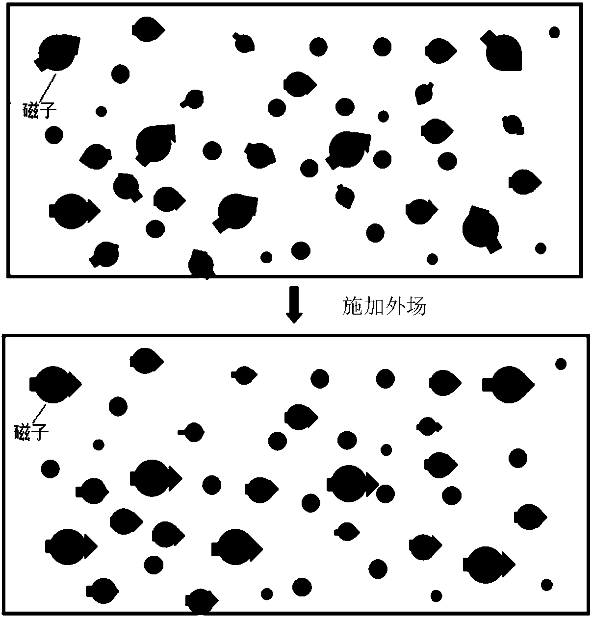
The invention belongs to the technical field of quantum dots, and particularly relates to an electrode and a QLED device. The electrode comprises an electrode material and a magnetic material, whereinthe electrode material is an anode material or a cathode material. The magnetic material in the electrode can adjust the carrier mobility; when the electrode material is an anode, the magnetic material can adjust the hole mobility, and when the electrode material is a cathode, the magnetic material can adjust the hole mobility, so that the injection balance of carriers is improved; and therefore,when the electrode is used for preparing the QLED device, the luminous efficiency and the stability of the device can be effectively improved.

Description

technical field [0001] The invention belongs to the technical field of quantum dots, and in particular relates to an electrode and a QLED device. Background technique [0002] Quantum Dot Light Emitting Diodes (Quantum Dot Light Emitting Diodes QLED) is a light-emitting device based on inorganic nanocrystal quantum dot materials. A strong contender for next-generation display technology. Usually in a multilayer structure QLED device, an important point affecting its luminous efficiency is the carrier balance problem. Usually, the movable holes reach the light-emitting layer from the anode through the hole injection and transport layer, and recombine with the electrons migrated from the cathode through the electron injection and transport layer to form excitons, and then the excitons radiate and emit photons. It is worth noting that too many holes or electrons will generate a three-particle system, which will cause the quenching of the generated excitons, thereby reducing t...

Claims


Application Information

Patent Timeline
Patent Type & Authority Applications(China)
IPC IPC(8): H01L51/52
CPCH10K50/115H10K50/81H10K50/82
Inventor 王雄志向超宇李乐张滔辛征航李雪
Owner TCL CORPORATION
Learn More