Quantum dot light emitting diode and preparation method thereof

A quantum dot light-emitting and diode technology, which is applied in semiconductor/solid-state device manufacturing, semiconductor devices, electrical components, etc., can solve the problem of insignificant aging effect of QLED devices, and is conducive to charge injection balance and suppression of surface exciton quenching. , the effect of increasing the probability of exciton radiation recombination

Pending Publication Date: 2022-07-01
TCL CORPORATION
View PDF1 Cites 0 Cited by
  • Summary
  • Abstract
  • Description
  • Claims
  • Application Information

AI Technical Summary

Problems solved by technology

[0005] The purpose of this application is to provide a quantum dot light-emitting diode and its preparation method, aiming to solve the problem that the positive aging effect on blue and red QLED devices is not obvious when using saturated / unsaturated carboxylic acid and other active materials to encapsulate the device

Method used


Image

  • Quantum dot light emitting diode and preparation method thereof
  • Quantum dot light emitting diode and preparation method thereof
  • Quantum dot light emitting diode and preparation method thereof

Examples


preparation example Construction

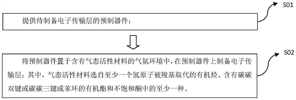
[0053] like figure 2 As shown, the first method for preparing a quantum dot light-emitting diode includes the following steps:

[0054] S01. Provide a prefabricated device with an electron transport layer to be prepared;

[0055] S02. The prefabricated device is placed in an atmosphere containing a gaseous active material, and an electron transport layer is prepared on the prefabricated device; wherein, the gaseous active material is selected from organic hydrocarbons with at least one hydrogen atom substituted by a carboxyl group, a carbon-carbon double bond or carbon At least one of organic esters of carbon triple bonds or benzene rings and unsaturated ketones.

[0056] In the above step S01, a prefabricated device with an electron transport layer to be prepared is provided. In one embodiment, the prefabricated substrate includes an anode substrate, and a quantum dot light-emitting layer combined on the anode surface of the anode substrate. In some embodiments, the prefa...

Embodiment 1

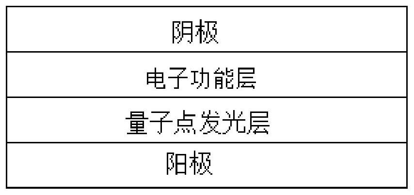
[0085] like Figure 4 As shown, a red quantum dot light-emitting diode, a substrate 100, an anode 110 located on the substrate 100, and a hole functional layer 120, a quantum dot light-emitting layer 130, an electron transport layer 140 and a cathode 150 are sequentially stacked, wherein The material of the substrate 100 is silicon glass, the material of the anode 110 is ITO, the material of the hole function layer 120 is TFB, the material of the quantum dot light-emitting layer 130 is CdZnSe / ZnSe / ZnS, the material of the electron transport layer is ZnO, and the material of the cathode is ZnO. The material of 150 is Ag.

[0086] A preparation method of a quantum dot light-emitting diode, comprising:

[0087] On the anode substrate, spin-coating the hole functional material to prepare the hole functional layer 120; spin-coating the quantum dot light-emitting material on the surface of the hole functional layer 120 to prepare the quantum dot light-emitting layer 130 to obtain a ...

Embodiment 2

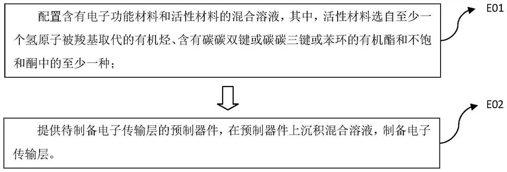
[0091] The difference from Example 1 is that in the process of preparing the red quantum dot light-emitting diode, the preparation method of the electron transport layer 140 is as follows:

[0092] According to the molar ratio of ZnO nanoparticles and acrylic acid to be 100:1, the mixed solution of active material and electron transport material is configured;

[0093] The mixed solution of the active material and the electron transport material is spin-coated on the obtained prefabricated device to prepare the electron transport layer 140 .


PUM


Abstract

The invention relates to the technical field of display, and provides a quantum dot light emitting diode and a preparation method thereof. The quantum dot light-emitting diode comprises an anode and a cathode which are oppositely arranged, a quantum dot light-emitting layer arranged between the anode and the cathode, and an electron transport layer arranged between the quantum dot light-emitting layer and the cathode. Wherein the electron transport layer contains an electron transport material and an active material, and the active material is selected from at least one of organic hydrocarbon with at least one hydrogen atom substituted by carboxyl, organic ester containing a carbon-carbon double bond or a carbon-carbon triple bond or a benzene ring, and unsaturated ketone. The positive aging effect of the quantum dot light-emitting diode is improved by introducing the active material into the electron transport layer.

Description

technical field [0001] The invention belongs to the technical field of display, and in particular relates to a quantum dot light-emitting diode and a preparation method thereof. Background technique [0002] Quantum Dot Light Emitting Diodes (QLED) are electroluminescent devices based on quantum dots (QDs) technology. A series of excellent characteristics such as flexible panels, good temperature characteristics, fast response speed, energy saving and environmental protection have become the research hotspot and key development direction of new display technology. [0003] Although QLED devices borrow and utilize the structure of organic light-emitting diodes (Organic Light-Emitting Diode, OLED), due to the difference in material composition, the aging phenomenon and aging mechanism of the two are very different. For example, QLED devices have various efficiencies (current, power or external quantum efficiency) that decay or increase over time, namely "negative aging effect...

Claims


Application Information

Patent Timeline
Patent Type & Authority Applications(China)
IPC IPC(8): H01L51/50H01L51/56
CPCH10K50/115H10K50/165H10K71/00
Inventor 王劲杨一行曹蔚然
Owner TCL CORPORATION
Why Eureka
Try Eureka