Quantum dot light emitting diode and preparation method thereof
A quantum dot light-emitting and diode technology, which is applied in the manufacture of semiconductor/solid-state devices, semiconductor devices, electrical components, etc., can solve the problems of QLED device aging effects, etc., to achieve balance of charge injection, increase recombination probability, and improve The effect of the aging effect
- Summary
- Abstract
- Description
- Claims
- Application Information
AI Technical Summary
Problems solved by technology
Method used
Image
Examples
preparation example Construction
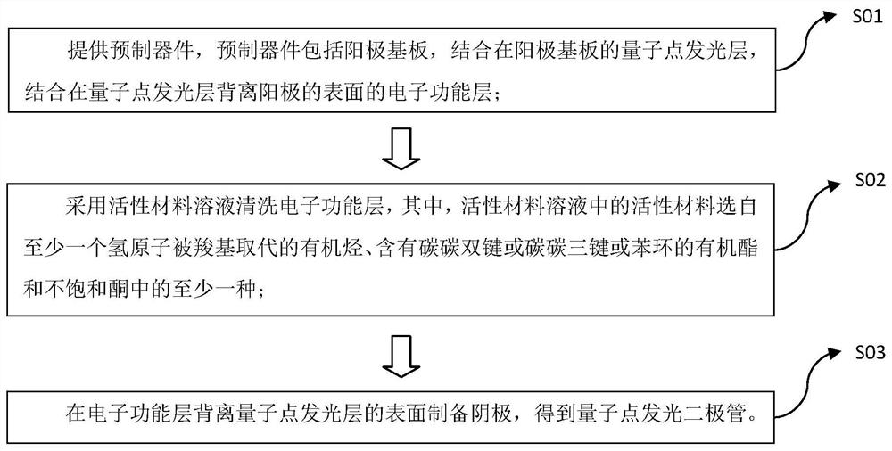
[0068] like figure 2 As shown, the first method for preparing a quantum dot light-emitting diode includes the following steps:
[0069] S01. Provide a prefabricated device, the prefabricated device includes an anode substrate, a quantum dot light-emitting layer combined on the anode substrate, and an electronic functional layer combined on the surface of the quantum dot light-emitting layer away from the anode;
[0070] S02. use active material solution to clean the electronic functional layer, wherein, the active material in the active material solution is selected from organic hydrocarbons with at least one hydrogen atom substituted by carboxyl groups, organic esters containing carbon-carbon double bonds or carbon-carbon triple bonds or benzene rings and at least one of unsaturated ketones;
[0071] S03. Prepare a cathode on the surface of the electronic functional layer away from the quantum dot light-emitting layer to obtain a quantum dot light-emitting diode.
[0072] ...
Embodiment 1
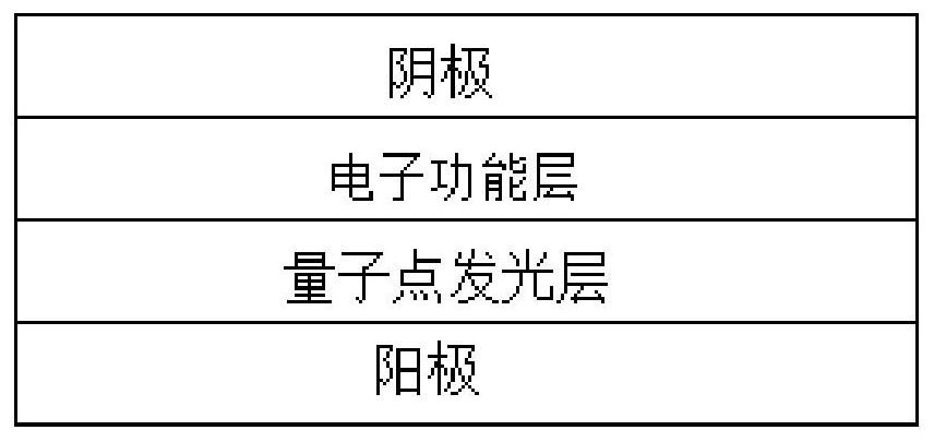
[0104] like Figure 5 As shown, a red quantum dot light-emitting diode, an anode 110 located on a substrate 100, and a hole functional layer 120, a quantum dot light-emitting layer 130, an electron functional layer 140 and a cathode 150 are stacked in sequence, wherein the substrate 100 The material is silicon glass, the material of the anode 110 is ITO, the material of the hole function layer 120 is TFB, the material of the quantum dot light-emitting layer 130 is CdZnSe / ZnSe / ZnS, the material of the electron function layer 140 is ZnO, and the material of the electron function layer 140 is ZnO. The surface of 140 adjacent to the cathode 150 is treated with acrylic acid, and the material of the cathode 150 is Ag.
[0105] A preparation method of a quantum dot light-emitting diode, comprising:
[0106] On the anode substrate, spin-coating a hole functional material to prepare a hole functional layer 120, and prepare a quantum dot light-emitting layer 130 on the hole functional l...
Embodiment 2
[0110] A red quantum dot light-emitting diode with the same composition and material as Example 1, the difference lies in the manner of "the surface of the electronic functional layer 150 is treated with acrylic acid". Specifically, the method of “the surface of the electronic functional layer 140 is treated with acrylic acid” in Example 2 is:
[0111] The resulting prefabricated device was placed in N 2 Or in an atmosphere composed of Ar and acrylic vapor for 20 minutes, the surface of the electronic functional layer 140 is treated with acrylic acid; wherein, the volume of acrylic acid accounts for 30% of the total gas volume, the temperature of the gaseous environment is 80 ° C, and the total pressure is 1 MPa .
PUM
| Property | Measurement | Unit |
|---|---|---|
| Thickness | aaaaa | aaaaa |
| Thickness | aaaaa | aaaaa |
| Volume concentration | aaaaa | aaaaa |
Abstract
Description
Claims
Application Information


