Cavity type bulk acoustic wave resonator with lower electrode protection layer and preparation method thereof
A technology of bulk acoustic wave resonators and protective layers, which is applied to electrical components, impedance networks, etc., can solve problems affecting device performance, electrode structure damage, etc., and achieve the effect of high quality factor and simple preparation method
- Summary
- Abstract
- Description
- Claims
- Application Information
AI Technical Summary
Problems solved by technology
Method used
Image
Examples
preparation example Construction
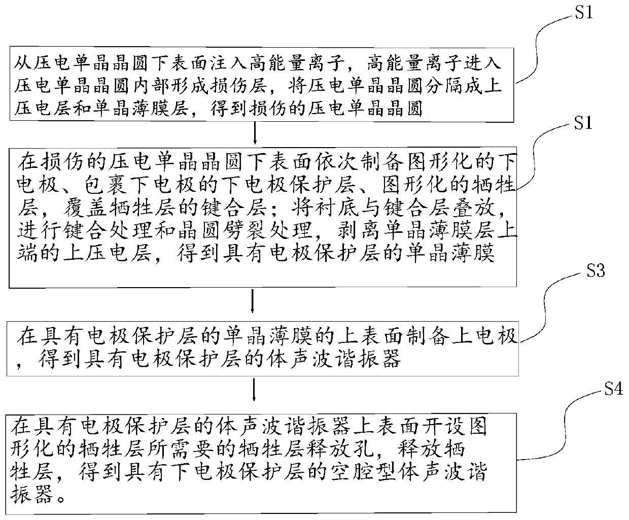
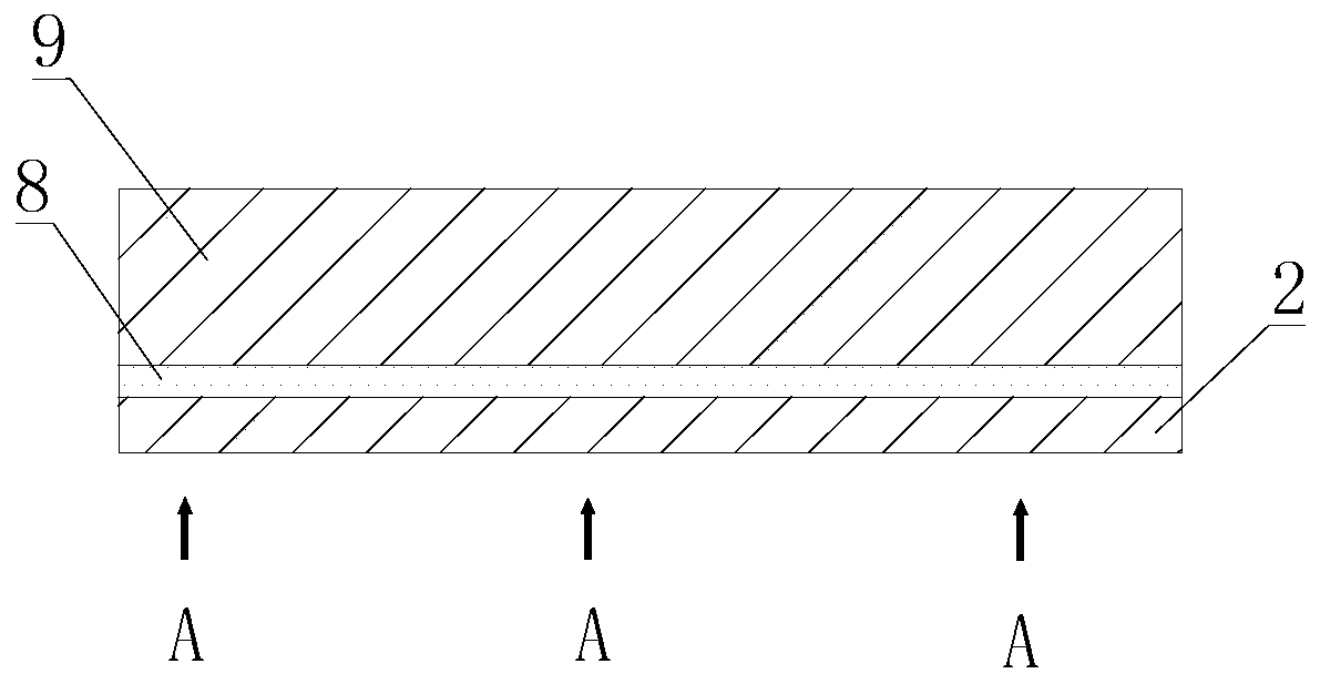
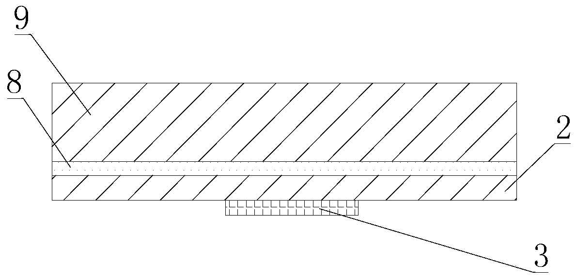
[0049] Such as figure 1 , figure 2 , image 3 , Figure 4 , Figure 5 , Figure 6 , Figure 7 , Figure 8 and Figure 9 As shown, a method for preparing a cavity-type bulk acoustic resonator with a lower electrode protective layer provided by the present invention includes the following steps:
[0050] S1) High-energy ions A are injected from the lower surface of the piezoelectric single-crystal wafer, and the high-energy ions A enter the interior of the piezoelectric single-crystal wafer to form a damaged layer 8, which separates the piezoelectric single-crystal wafer into an upper piezoelectric layer 9 and a single piezoelectric layer 9. crystal thin film layer 2 to obtain a damaged piezoelectric single crystal wafer;
[0051] S2) sequentially prepare a patterned lower electrode 3, a lower electrode protective layer 4 wrapping the lower electrode, a patterned sacrificial layer 10, and a bonding layer 5 covering the sacrificial layer on the lower surface of the damag...
Embodiment 1
[0073] 1) Select a lithium niobate piezoelectric single crystal wafer, and inject high-energy He into the lower surface of the lithium niobate piezoelectric single crystal wafer + , so that a damaged layer is formed inside the lithium niobate piezoelectric single crystal wafer, and the damaged layer separates the lithium niobate piezoelectric single crystal wafer into a lithium niobate upper piezoelectric layer and a lithium niobate single crystal thin film layer; He + The implantation energy is 200keV, and the implantation depth is 0.6μm.
[0074] 2) The lower electrode is prepared on the lower surface of the lithium niobate single crystal thin film layer. The lower electrode can be prepared in two ways. The first method is to coat the lower surface of the lithium niobate single crystal thin film layer with photoresist (Ruihong AZ6212), forming a photoresist layer, using a patterned mask plate (made of chromium) to expose the photoresist, developing with a developer, growing ...
Embodiment 2
[0081] 1) Select a lithium tantalate piezoelectric single crystal wafer, and inject high-energy He into the lower surface of the lithium niobate piezoelectric single crystal wafer + , so that a damaged layer is formed inside the lithium niobate piezoelectric single crystal wafer, and the damaged layer separates the lithium niobate piezoelectric single crystal wafer into a lithium niobate upper piezoelectric layer and a lithium niobate single crystal thin film layer; He + The implantation energy is 500keV, and the implantation depth is 0.6μm.
[0082] 2) The lower electrode is prepared on the lower surface of the lithium tantalate single crystal thin film layer. The lower electrode can be prepared in two ways. The first method is to coat the lower surface of the lithium tantalate thin film layer with photoresist (Ruihong AZ6212), forming a photoresist layer, using a patterned mask plate (made of chromium) to expose the photoresist, developing with a developer, growing the lower...
PUM
 Abstract
Description
Claims
Application Information


