SIP module partition electromagnetic shielding package method

A technology of electromagnetic shielding and packaging method, applied in the manufacturing of circuits, electrical components, semiconductor/solid-state devices, etc., can solve the problems of reducing cost, increasing the substrate area, disadvantage, etc., saving process technology, improving reliability, and saving costs Effect

Inactive Publication Date: 2019-07-12
中电海康无锡科技有限公司
View PDF9 Cites 7 Cited by
  • Summary
  • Abstract
  • Description
  • Claims
  • Application Information

AI Technical Summary

Problems solved by technology

The main problem in doing this is that the slot between the two chips must be large enough. Taking the general SIP as an example (thickness less than 1mm), the filling generally needs to be slotted to more than 300 microns, plus the distance from the chip to the edge of the plastic package, the chip The distance between them is basically 600 microns, so these special requirements need to be considered in the design. Increase the distance design for the chips that need to be shielded, resulting in an increase in the substrate area, which is not conducive to reducing costs.

Method used


Image

  • SIP module partition electromagnetic shielding package method
  • SIP module partition electromagnetic shielding package method
  • SIP module partition electromagnetic shielding package method

Examples


Embodiment Construction

[0024] The present invention will be further described below in conjunction with specific drawings and embodiments.

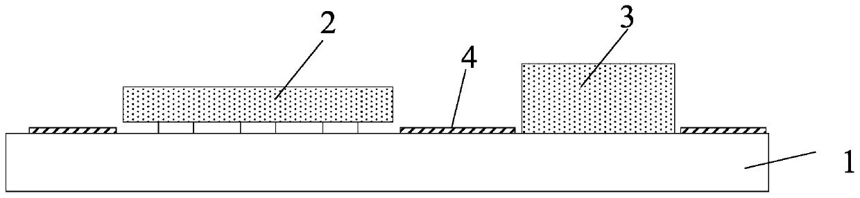
[0025] In step S1, a substrate 1 is provided, and the flip chip 2 and the passive component 3 are mounted on the first working surface of the substrate 1, and there are prefabricated grounding pads around the chip mounting position on the first working surface of the substrate 1. 4;

[0026] Among them, chip 2 is mounted by flip-chip welding;

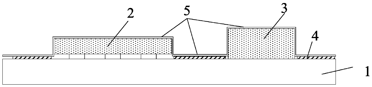
[0027] Step S2, then first perform plasma surface cleaning (Plasma surface cleaning) on ​​the substrate 1, then use a vacuum lamination (Lamination) machine, and then perform film plastic sealing on the first working surface of the substrate 1 to form a cover on the first working surface of the substrate 1 plastic film 5;

[0028] Thus, the chip 2, the passive element 3, and the ground pad 4 are all covered by the plastic film 5;

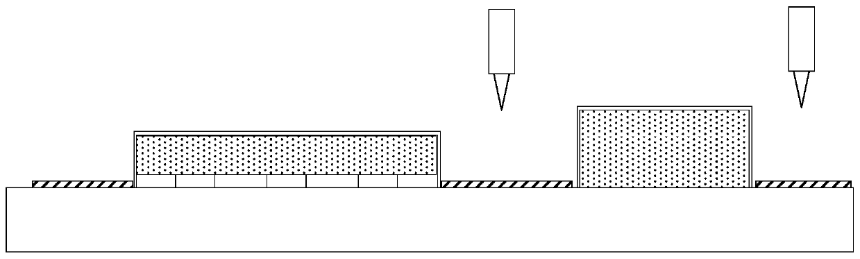
[0029] Step S3, using a laser to make grooves around the chips that need partition shie...


PUM


Abstract

The invention provides a SIP (System In Package) module partition electromagnetic shielding package method. The method comprises the steps of: providing a substrate, mounting a flip chip and a passiveelement at the first working surface of the substrate, wherein manufactured grounding bonding pads are arranged at the periphery of the chip mounting position of the first working surface of the substrate; performing plasma surface cleaning for the substrate, performing thin film plastic package for the first working surface of the substrate to form a plastic package film covering the first working surface of the substrate; employing a laser to perform slotting around the chip requiring partition shielding to expose the corresponding grounding bonding pads; performing sputtering for the firstworking surface of the whole substrate to form an inner metal shielding layer and achieve chip partition shielding; performing plasma cleaning for the substrate after sputtering, and performing plastic package for the first surface of the substrate to form an outer package body; and cutting the whole substrate to form each single SIP module. The SIP module partition electromagnetic shielding package method facilitates reduction of the module size, improves the reliability and improves the production efficiency.

Description

technical field [0001] The invention relates to the technical field of integrated circuit packaging, in particular to a SIP module partition electromagnetic shielding packaging method. Background technique [0002] As the integration density of SIP modules (System In Package) becomes higher and higher, the products become more and more complex. Previously, the metallization shielding technology on the product surface can only solve the problem of electromagnetic interference between modules, but it is no longer able to meet the requirements inside the module. The problem of electromagnetic interference between chips, so mainstream manufacturers are developing related partition shielding technology. [0003] At present, the partition shielding technology used by SIP modules basically uses laser to dig grooves between the chips that need to be shielded after the plastic packaging is completed, and then fills the conductive material between the plastic packaging materials, and ...

Claims


Application Information

Patent Timeline
Patent Type & Authority Applications(China)
IPC IPC(8): H01L21/56
CPCH01L21/56H01L21/563
Inventor 林江宽孟涛
Owner 中电海康无锡科技有限公司
Why Eureka
Try Eureka