Mobile phone shell with optical microstructure textures and processing method
A technology of microstructure texture and optical microstructure, applied in the direction of telephone structure, telephone communication, electrical components, etc., can solve the problems of height, corner radius and draft angle limitation, no side wall height, etc., to reduce production costs , Improve the yield and the effect of high production precision
- Summary
- Abstract
- Description
- Claims
- Application Information
AI Technical Summary
Problems solved by technology
Method used
Image

Examples
Embodiment 1
[0105] This embodiment proposes a mobile phone case with optical microstructure texture and a manufacturing process of the mobile phone case. This process lacks a layer of micro-structure film, but directly builds the micro-nano structure on the mobile phone case, for example, processing the micro-nano structure on the inner side of the mobile phone case, and then passing through transparent optical glue, reflective film, and black glue. combined.
[0106] The microstructure texture is one-dimensional, two-dimensional periodic array microstructure texture; one-dimensional gradient, two-dimensional gradient microstructure texture; ring, spiral, quadrilateral, hexagonal, polygonal microstructure arrangement Texture; Fresnel pattern, ring pattern (CD pattern) microstructure texture with zoom-in and zoom-out characteristics visually, retro-reflective corner cube prism microstructure texture; and other micro-nano structure composition on the surface of bionic and imitation objects....
Embodiment 2
[0122] This embodiment discloses a mobile phone case with an optical microstructure texture. In addition to coating the reflective paint layer on the surface of the microstructure as described in the first specific embodiment, it can be provided with a separate reflective film, as described in the second specific embodiment. stated.
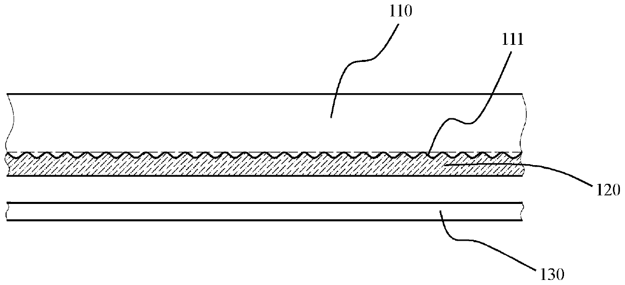
[0123] The partial sectional view of its specific embodiment is as Figure 8 shown. It consists of a plastic housing 210 , a transparent optical adhesive (OCA) 230 , a reflective film 240 , and a black adhesive 250 .
[0124] The plastic shell 210 is made of PC, ABS, PET, nylon or PMMA, and its thickness is 0.4-0.6mm, preferably 0.5mm; the transparent optical adhesive (OCA) 230, its thickness is 24-26nm, Preferably 25nm; the reflective film 240, which is coated with a color (such as blue or gradient color), has a thickness of 8-15nm; the black glue 250 is an oil film layer, and its thickness is 14-16nm, preferably 15nm.
[0125] The inner surf...
Embodiment 3
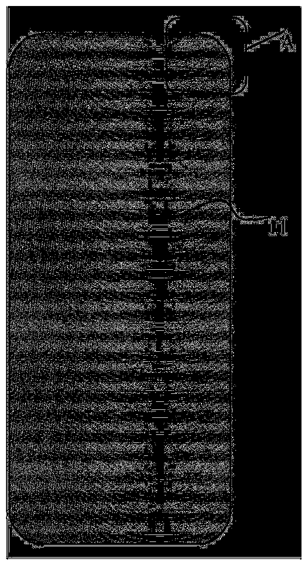
[0130] This embodiment discloses a mobile phone case with an optical microstructure texture. The plastic casing has a periodic microstructure texture provided on its inner surface. It may be an arc or a periodic grating structure of high and low bosses / grooves, as described in this specific embodiment.
[0131] The mobile phone shell with optical microstructure texture described in this embodiment, the inner surface of the plastic shell is provided with a periodic microstructure texture of straight high and low protrusions / grooves, and its partial enlarged view is as follows Figure 9 shown. It is perpendicular to the C-C direction of the texture, together with the structural schematic diagram of the underlying multilayer film, such as Figure 10 shown. It is formed by laminating a plastic shell 310 , a transparent optical adhesive (OCA) 330 , a reflective film 340 , and a black adhesive 350 .
PUM
| Property | Measurement | Unit |
|---|---|---|
| Thickness | aaaaa | aaaaa |
| Thickness | aaaaa | aaaaa |
| Depth | aaaaa | aaaaa |
Abstract
Description
Claims
Application Information
 - R&D
- Intellectual Property
- Life Sciences
- Materials
- Tech Scout
- Unparalleled Data Quality
- Higher Quality Content
- 60% Fewer Hallucinations
Browse by: Latest US Patents, China's latest patents, Technical Efficacy Thesaurus, Application Domain, Technology Topic, Popular Technical Reports.
© 2025 PatSnap. All rights reserved.Legal|Privacy policy|Modern Slavery Act Transparency Statement|Sitemap|About US| Contact US: help@patsnap.com