

A Terahertz Detector Based on Antiferromagnetic Nonmagnetic Metal Heterojunction
A terahertz detector and antiferromagnetic technology, which is applied in photometry using electric radiation detectors, metal material coating technology, vacuum evaporation plating, etc., can solve the problems of lack of terahertz detection technology and achieve zero work consumption, fast response, and easy integration
- Summary
- Abstract
- Description
- Claims
- Application Information
AI Technical Summary
Problems solved by technology
Method used
Image

Examples
Embodiment 1
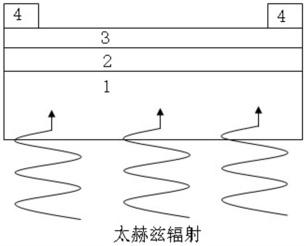
[0016] Spin-coat photoresist on a 4-inch high-resistance silicon substrate, and photoetch many pieces of 1x2mm 2 Then put it into the magnetron sputtering deposition chamber to prepare NiO antiferromagnetic material on it. When sputtering the antiferromagnetic material, add a magnetic field with an intensity of 1000Oe parallel to the substrate surface, and the direction of the magnetic field is vertical. on the long side of the small rectangular block. The thickness of the antiferromagnetic layer is 3nm. Then proceed to deposit a non-magnetic metal Pt layer with a thickness of 3nm. Take out the sample for degumming, spin-coat photoresist again, and photoetch 1x0.5mm on both sides of the small rectangle 2 Then put the sample into the magnetron sputtering deposition chamber again to deposit a gold electrode with a thickness of 200nm. Take out the samples for degumming, cleaning, cutting, spot welding of leads, and packaging to complete the production of the detector.
Embodiment 2
[0018] Spin-coat photoresist on a 4-inch high-resistance silicon substrate, and photoetch many pieces of 1x2mm 2 The size of the blank rectangular area, and then placed in the magnetron sputtering deposition chamber on which to prepare Cr 2 o 3 For the antiferromagnetic material, a magnetic field with a strength of 1000Oe parallel to the substrate surface is applied when the antiferromagnetic material is deposited by sputtering, and the direction of the magnetic field is perpendicular to the long side of the small rectangular block. The thickness of the antiferromagnetic layer is 30nm. Then continue to deposit a non-magnetic metal W layer with a thickness of 30nm. Take out the sample for degumming, spin-coat photoresist again, and photoetch 1x0.5mm on both sides of the small rectangle 2 Then put the sample into the magnetron sputtering deposition chamber again to deposit a gold electrode with a thickness of 200nm. Take out the samples for degumming, cleaning, cutting, spot...
Embodiment 3
[0020] Spin-coat photoresist on a 4-inch high-resistance silicon substrate, and photoetch many pieces of 1x2mm 2 The blank rectangular area of the size is then put into the magnetron sputtering deposition chamber to prepare BiFeO on it 3 For the antiferromagnetic material, a magnetic field with a strength of 1000Oe parallel to the substrate surface is applied when the antiferromagnetic material is deposited by sputtering, and the direction of the magnetic field is perpendicular to the long side of the small rectangular block. The thickness of the antiferromagnetic layer is 300nm. Then proceed to deposit a non-magnetic metal Pd layer with a thickness of 300nm. Take out the sample for degumming, spin-coat photoresist again, and photoetch 1x0.5mm on both sides of the small rectangle 2 Then put the sample into the magnetron sputtering deposition chamber again to deposit a gold electrode with a thickness of 200nm. Take out the samples for degumming, cleaning, cutting, spot wel...
PUM
| Property | Measurement | Unit |
|---|---|---|
| thickness | aaaaa | aaaaa |
| thickness | aaaaa | aaaaa |
| thickness | aaaaa | aaaaa |
Abstract
Description
Claims
Application Information