A kind of semiconductor storage device and computer system

A storage device and semiconductor technology, applied in information storage, static storage, digital storage information, etc., can solve problems such as performance defects and limit storage capacity, and achieve the effect of improving service life, improving storage performance, and shortening IO paths.

Active Publication Date: 2020-07-03
江苏数一互联网有限公司
View PDF9 Cites 0 Cited by
  • Summary
  • Abstract
  • Description
  • Claims
  • Application Information

AI Technical Summary

Problems solved by technology

However, under the configuration of solid-state storage media (such as NAND memory), the storage performance of the Ceph cluster is only about 40% of the hardware limit performance, which greatly limits the storage capacity of the computer system or the cloud platform based on the computer system. , especially when reading large files, there are certain performance defects

Method used


Image

  • A kind of semiconductor storage device and computer system
  • A kind of semiconductor storage device and computer system
  • A kind of semiconductor storage device and computer system

Examples


Embodiment 1

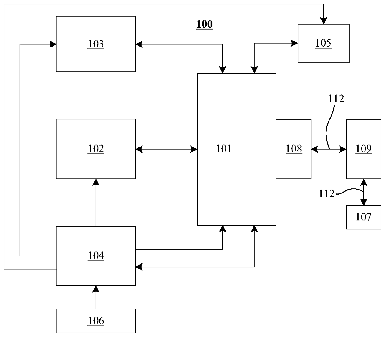
[0030] ginseng figure 1 As shown, this embodiment discloses a semiconductor storage device 100, the semiconductor storage device 100 is connected to the host 107 through the system bus 112, including:

[0031] The volatile memory 103 , the first non-volatile memory 102 , and the storage controller 101 communicate with the host 107 through the interface module 108 . The storage controller 101 responds to the power signal and the control signal of the host 107 and alternatively performs data access operations with the volatile memory 103 or the first non-volatile memory 102 .

[0032] In this embodiment, the semiconductor storage device 100 further includes a second non-volatile memory 105 connected to the storage controller 101, and the storage controller 10 stores the power state data in the form of power state data according to the power signal of the host computer 107. For the second non-volatile memory 105, a kernel bypass module 109 is set between the memory controller 10...

Embodiment approach

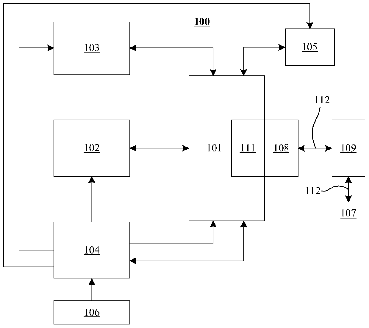
[0047] ginseng figure 2 Shown is a second specific implementation manner of a semiconductor storage device 100 of the present invention. Compared with the first embodiment, the semiconductor storage device 100 disclosed in this embodiment differs mainly in that in this embodiment, the storage controller 101 is configured with an MMAP interface 111 and communicates with the interface module 108 through the MMAP interface 111 .

[0048] When the computer system crashes abnormally or loses power abnormally, the data in the volatile memory 103 will be lost. For applications with high data consistency requirements, such as databases, it may be a fatal blow. In order to solve the above problems, in this embodiment, by setting the MMAP interface 111, the application program is provided with direct access to the logic blocks in the volatile memory 103 as accessing common memory, thereby bypassing the operating system page cache mechanism and improving The access efficiency of the ...

Embodiment 3

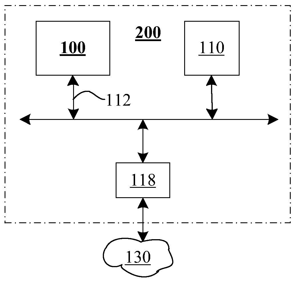
[0052] As shown in reference 3, this embodiment discloses a computer system. A computer system disclosed in this embodiment may include one or more semiconductor storage devices 100 disclosed in Embodiment 1 or Embodiment 2 or a combination of both.

[0053] The computer system 200 includes: a processor 110 , and a semiconductor storage device 100 connected to a host 107 through a system bus 112 . The semiconductor storage device 100 includes a volatile memory 103, a first non-volatile memory 102, a storage controller 101 communicating with a host 107 through an interface module 108, and the storage controller 101 responds to the power signal of the host 107 and control signals, and alternatively perform data access operations with the volatile memory 103 or the first non-volatile memory 102 .

[0054] The semiconductor storage device 100 also includes a second non-volatile memory 105 connected to the storage controller 101, and the storage controller 10 saves to the second non...


PUM


Abstract

The invention provides a semiconductor storage device and a computer system. The semiconductor storage device is connected to a host through a system bus, and includes a volatile memory, a first non-volatile memory, and a storage controller. The storage controller responds to the power supply of the host signals and control signals, and alternatively perform data access operations with the volatile memory or the first non-volatile memory, and the second non-volatile memory connected to the storage controller, the storage controller according to the host The power signal is stored in the second non-volatile memory in the form of power state data, and a kernel bypass module is set between the memory controller and the host. In the present invention, the power state data can be written into the second non-volatile memory when the computer is normally shut down, so as to avoid frequently writing the power state data into the first non-volatile memory, thereby significantly improving The service life of the first nonvolatile memory in the semiconductor memory device is extended.

Description

technical field [0001] The invention relates to the technical field of semiconductor storage, in particular to a semiconductor storage device with an emergency backup function applied to a computer in case of unexpected power failure, and a computer system based on the semiconductor storage device. Background technique [0002] With the continuous development of semiconductor device manufacturing technology, the line width and frequency of central processing unit (CPU) and memory (Memory) have been greatly increased, and the IO bottleneck problem of traditional mechanical hard disk (HDD) is increasingly restricting the improvement of computer performance. , So people began to use flash memory (FLASH) instead of HDD. Flash memory generally adopts a single-level cell structure (Single-level cell, SLC) or a multi-level cell structure (Multi-level Cell, MLC). However, the manufacturing cost of SLC flash memory is generally high, so MLC flash memory is usually used at present, b...

Claims


Application Information

Patent Timeline
Patent Type & Authority Patents(China)
IPC IPC(8): G11C14/00
CPCG11C14/00
Inventor 万胤岳周介龙
Owner 江苏数一互联网有限公司
Why Eureka
Try Eureka