Low-damage AlGaN/GaN HEMT gate groove etching method

A low-damage, gate-trough technology, used in semiconductor/solid-state device manufacturing, electrical components, circuits, etc., can solve problems such as inability to accurately control the etching accuracy, large surface damage to the etched sample, and uneven sample etching. Achieve the effect of reducing roughness, reducing bombardment, and reducing surface damage

Active Publication Date: 2019-07-23
JIANGNAN UNIV
View PDF8 Cites 4 Cited by
  • Summary
  • Abstract
  • Description
  • Claims
  • Application Information

AI Technical Summary

Problems solved by technology

[0005] In order to solve the problems that the existing etching technology has a large damage to the surface of the etching sample, which is easy to be broken down, the etching surface of the sample is uneven, and the etching precision cannot be accurately controlled, the present invention proposes a low-damage AlGaN / GaN HEMT gate groove The etching method, the low-damage AlGaN / GaNHEMT gate groove etching method provided by the present invention, is based on the mild plasma technology;

Method used


Image

  • Low-damage AlGaN/GaN HEMT gate groove etching method
  • Low-damage AlGaN/GaN HEMT gate groove etching method
  • Low-damage AlGaN/GaN HEMT gate groove etching method

Examples


Embodiment 1

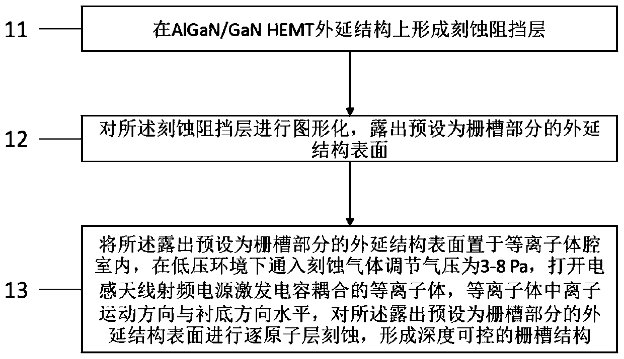
[0036] This embodiment provides a low-damage AlGaN / GaNHEMT gate groove etching method, see figure 1 , the method includes:

[0037] Step 11, forming an etching barrier layer on the AlGaN / GaN HEMT epitaxial structure;

[0038] Step 12, patterning the etching barrier layer to expose the surface of the epitaxial structure preset as the gate groove;

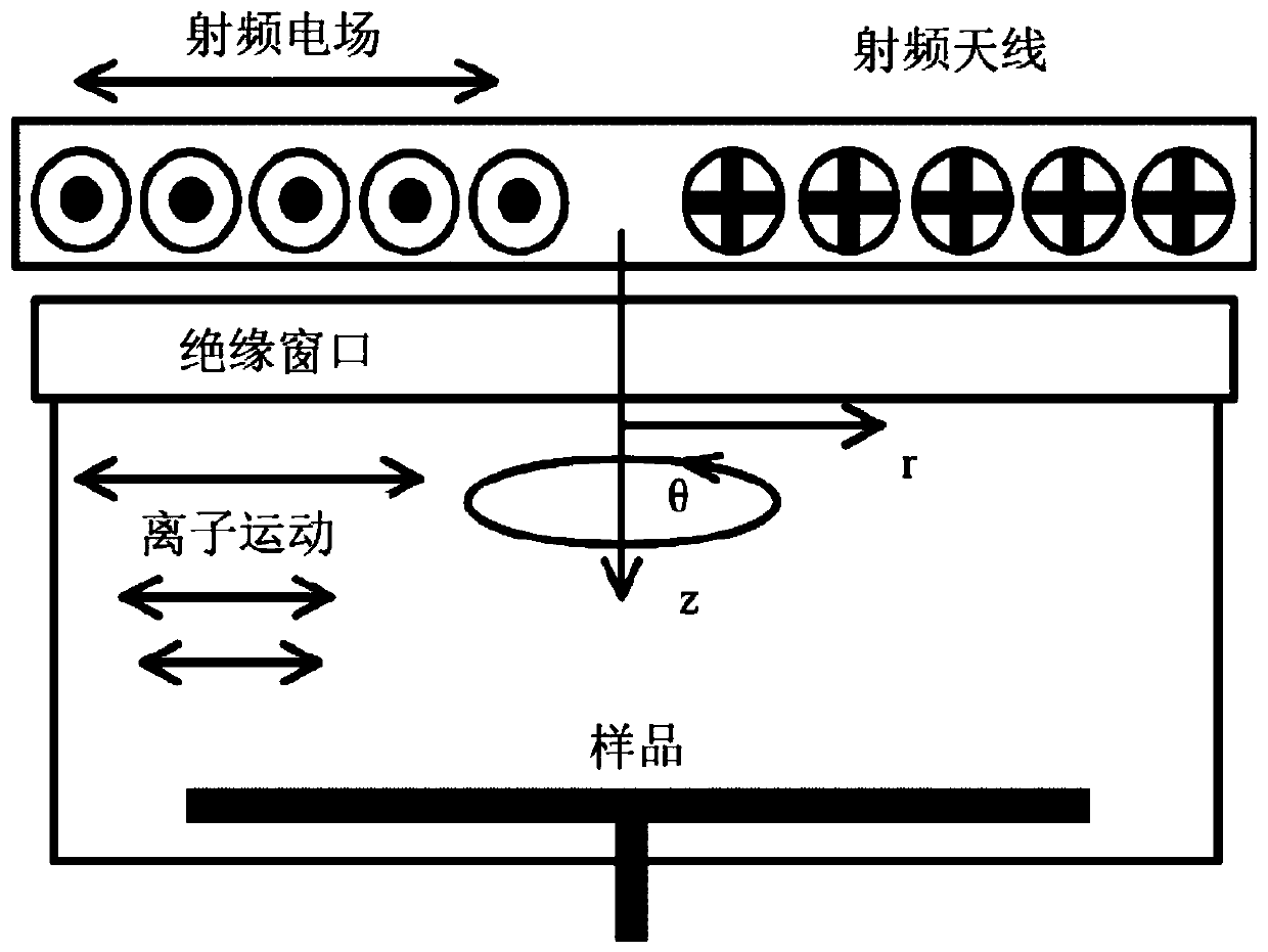
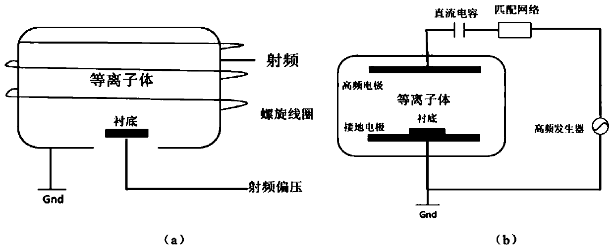
[0039] Step 13, placing the surface of the epitaxial structure exposed and preset as the gate groove in the plasma chamber, feeding etching gas in a low-pressure environment to adjust the pressure to 3-8Pa, and turning on the radio frequency power supply of the inductive antenna to excite capacitively coupled plasma , the moving direction of ions in the plasma is parallel to the direction of the substrate, and the surface of the epitaxial structure that is exposed and preset as the gate groove is etched atomically layer by atom to form a gate groove structure with a controllable depth.

[0040]The low-damage AlGaN / GaN HEMT gate gro...


PUM


Abstract

The invention discloses a low-damage AlGaN GaN HEMT gate groove etching method, and belongs to the technical field of semiconductor manufacturing. In the etching process of the method, the movement direction of ions in plasma is controlled to be horizontal to the direction of a substrate, and the concentration of the plasma is controlled to be 108-1010 cm<3>, the etching uniformity is improved, the roughness of an etching surface is reduced, the bombardment of the plasma on the surface of a sample is reduced to the minimum, the purpose of reducing surface damage is achieved, meanwhile, the etching rate can be reduced to 2-3 nm / min, and the etching precision is controlled accurately in the etching process.

Description

technical field [0001] The invention relates to a low-damage AlGaN / GaNHEMT gate groove etching method, which belongs to the technical field of semiconductor manufacturing. Background technique [0002] GaN HEMT devices have good application prospects in GaN-based integrated circuits in harsh environments due to their wide bandgap characteristics, good high-temperature characteristics and radiation resistance characteristics. However, due to the large difference in the mobility of holes and electrons in GaN, it is still difficult to prepare complementary symmetrical GaN field effect transistor circuit units in a CMOS-like manner, regardless of the device planar structure or device operating speed. A feasible method is to develop the turn-on and turn-off of n-type GaN enhancement devices that require a positive gate voltage to open the channel, which can realize GaN high-power switching devices and circuits, as well as enhancement / depletion mode digital integrated circuits. U...

Claims


Application Information

Patent Timeline
Patent Type & Authority Applications(China)
IPC IPC(8): H01L21/3065H01L21/67H01L21/28H01L21/335H01L29/423
CPCH01L29/66462H01L29/401H01L21/3065H01L29/4236H01L21/67248
Inventor 陈雷雷闫大为赵琳娜顾晓峰
Owner JIANGNAN UNIV
Why Eureka
Try Eureka