OLED display panel and manufacturing method thereof

A technology for display panels and manufacturing methods, which is applied in semiconductor/solid-state device manufacturing, semiconductor devices, electrical components, etc., and can solve problems such as high manufacturing costs, low production capacity, and difficulty in improving yields

Active Publication Date: 2021-07-06
SHENZHEN CHINA STAR OPTOELECTRONICS SEMICON DISPLAY TECH CO LTD
View PDF6 Cites 0 Cited by
  • Summary
  • Abstract
  • Description
  • Claims
  • Application Information

AI Technical Summary

Problems solved by technology

However, higher-precision masks and precise alignment are required in the manufacture of high-resolution displays, resulting in lower production capacity and higher costs; and the existing OLED display panels have a large number of structural layers, such as light-shielding layers and flat layers. , pixel definition layer, etc., it is difficult to improve the yield rate, and the patterning of these film layers also requires more masks, more complicated processes, and higher production costs

Method used


Image

  • OLED display panel and manufacturing method thereof
  • OLED display panel and manufacturing method thereof
  • OLED display panel and manufacturing method thereof

Examples


Embodiment Construction

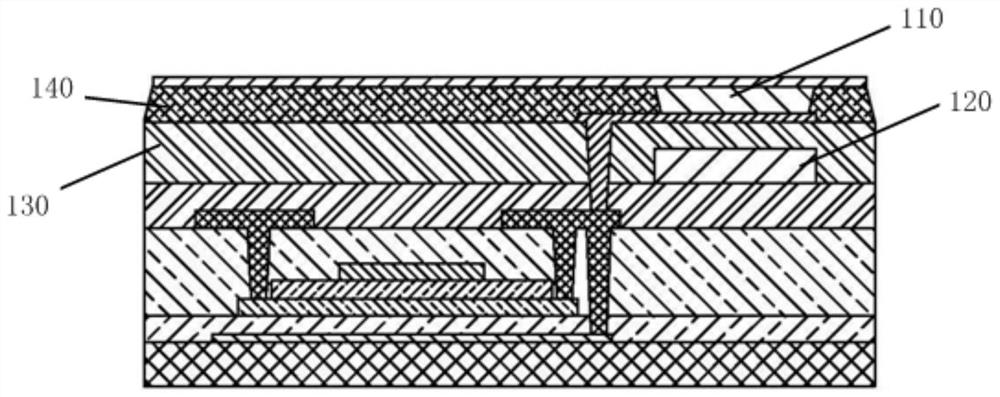
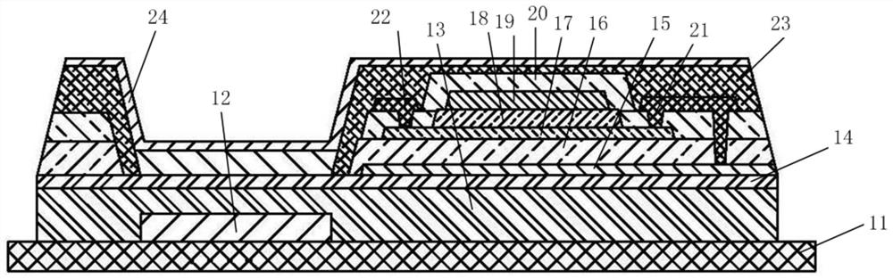
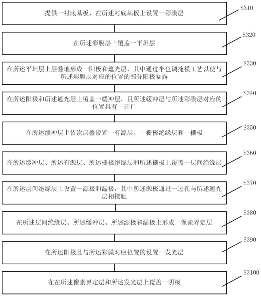
[0023] The following will clearly and completely describe the technical solutions in the embodiments of the present invention with reference to the drawings in the embodiments of the present invention. Apparently, the described embodiments are only some of the embodiments of the present invention, but not all of them. Based on the embodiments of the present invention, all other embodiments obtained by those skilled in the art without creative efforts fall within the protection scope of the present invention.

[0024] The terms "first", "second", "third", etc. (if any) in the description and claims of the present invention and the above drawings are used to distinguish similar objects and not necessarily to describe a specific order or sequentially. It should be understood that the items so described are interchangeable under appropriate circumstances. Furthermore, the terms "comprising" and "having", as well as any variations thereof, are intended to cover a non-exclusive in...


PUM


Abstract

The invention discloses an OLED display panel and a manufacturing method thereof. The OLED display panel adopts a top-gate emitting device, which only needs 8-11 yellow light processes. Compared with the existing 13 yellow light process, the present invention can reduce 2-5 processes. The number of masks, production time, and production consumables are all greatly reduced, thereby greatly reducing the production cost of vapor-deposited OLED display panels.

Description

technical field [0001] The invention relates to the field of display technology, in particular to an OLED display panel and a manufacturing method thereof. Background technique [0002] In the field of display technology, flat panel display devices such as liquid crystal display panels and organic light emitting diode display panels have gradually replaced cathode ray tube displays. [0003] Among them, the OLED display panel has many advantages such as self-illumination, low driving voltage, low luminous efficiency, short response time, high definition and contrast, nearly 180-degree viewing angle, wide operating temperature range, flexible display and large-area full-color display, etc. , is recognized by the industry as the display device with the most development potential. [0004] figure 1 It is a structural schematic diagram of an OLED display panel in the prior art. The common method of making OLED display panels is to deposit red, green and blue resist layers thr...

Claims


Application Information

Patent Timeline
Patent Type & Authority Patents(China)
IPC IPC(8): H01L27/32H01L51/56H01L27/12
CPCH01L27/1288H10K59/12H10K71/00
Inventor 何昆鹏任章淳
Owner SHENZHEN CHINA STAR OPTOELECTRONICS SEMICON DISPLAY TECH CO LTD
Why Eureka
Try Eureka